F6 A Fully Functional Mini RISC-V Processor
We have already implemented the sCPU, which can calculate the sum of 1+2+...+10. Although implementing this processor has indeed given us a deeper understanding of how processors work, from a practical perspective, the sCPU cannot run more complex programs due to various limitations. In fact, these limitations ultimately stem from the simplicity of the sISA instruction set, such as:
- The PC register has a width of only 4 bits, which means that a program can contain at most 16 instructions.
- The GPRs have a width of only 8 bits, making it impossible to represent data larger than 255.
- The functionality of instructions is limited; for example, it cannot perform subtraction operations, let alone multiplication and division.
Next, you will implement a fully functional RISC-V processor that can run more programs and even has the potential to run Super Mario!
Mini RISC-V Instruction Set
RISC-V is an open instruction set architecture that has gained prominence over the past decade. It employs a modular design philosophy, partitioning instructions into distinct subsets. Beyond the base instruction set RV32I, various extensions exist—including multiply/divide (M), floating-point (F), and atomic operations (A). Developers can selectively implement zero or more extensions based on application requirements. This flexibility has made it highly popular among developers.
The RV32I base set comprises 42 instructions. Implementing RV32I alone suffices for most computational tasks. To further reduce development effort, we propose minirv—a 'miniature RISC-V' instruction subset. Minirv selects 8 core instructions from RV32I that can functionally substitute all other RV32I instructions via instruction combinations. Consequently, any task achievable with RV32I can be executed using minirv. This approach eliminates the need to implement the full 42-instruction RV32I set while enabling processors to execute relatively complex programs.
As an actual Instruction Set Architecture,the details of the RISC-V specification are documented in corresponding official manuals. We encourage everyone to cultivate the good habit of reading official manuals. Therefore, you need to download the riscv manual. If this is your first exposure to ISA and processor design concepts, you may find it challenging to comprehend every detail in the manuals. However, we will guide you to locate key RV32I-related information within these documents.
Preliminarily understand the RISC-V instruction set through RTFM
Check the table of contents of the RISC-V manual. In which chapter is RV32I introduced? Try to look up the relevant content of RV32I in that chapter and answer the following questions:
- What is the bit width of the PC register?
- How many GPRs are there in total? What is the bit width of each GPR?
- What are the differences between
R[0]andR[0]in sISA? - What is the bit width of instruction encoding? How many basic formats do instructions have?
- In the basic format of instructions, how many bits are needed to represent a GPR? Why?
- What is the specific format of the
addinstruction? - There is another base instruction set called RV32E. What is the difference between it and RV32I?
After understanding some details of the RISC-V instruction set, we can present the specification of the ISA named minirv, as follows:
- The initial value of PC is
0. - The number of GPRs is the same as that defined in RV32E.
- It supports the following 8 instructions:
add,addi,lui,lw,lbu,sw,sb,jalr - Other ISA details are the same as those of RV32I.
A minirv processor with only two instructions
minirv has 8 instructions, and we will first implement two of them: addi , jalr. First, let's consider the addi instruction.
RTFM(2)
Consult the RISC-V manual to find the encoding and corresponding functional description of the addi instruction. There are some instruction tables in Chapter 34, "RV32/64G Instruction Set Listings", which can help you look up the encoding of the addi instruction.
For the instruction fetch process, you need to modify the width of the ROM and the bit width of the PC register. You have previously used gate circuits to build multiplexers and already understand the circuit structure of multiplexers. Building larger multiplexers is just repetitive engineering work and is not significantly helpful for learning. Therefore, we recommend that you use the Multiplexer component provided by Logisim. You can find it under the Plexers category in the component library, and after instantiation, you can easily adjust various parameters. Similarly, you can also find the Register under the Memory category in the component library, which is used to conveniently implement the PC register. For the specific usage of these two components, please RTFM. However, the concept of memory exists at both the circuit level and the ISA level. How to implement memory at the ISA level through memory at the circuit level has become a problem that needs to be considered.
RTFM(3)
To understand several conventions of RISC-V regarding memory, you need to read the first paragraph of Section 1.4 in the RISC-V manual, so as to understand the specifications of memory from the ISA level, especially the definition of width.
For ease of description, we refer to the memory width defined in the RISC-V manual as . Obviously, at the ISA level, the PC register addresses in units of . However, at the circuit level, if the width of the ROM is inconsistent with .The PC value cannot be directly used to address the ROM. You need to think about how to solve this problem at the circuit level.
For the decoding process, first consider the decoding of the opcode. Although there are decoders in the Logisim component library, since there are not many instructions in minirv, the opcode encoding is relatively sparse, and using a decoder will bring some inconvenience instead. Therefore, we recommend that you use a comparator. Decoding is performed by directly comparing whether the opcode field in the instruction is consistent with the encoding of the addi instruction. For example, you can determine whether an instruction is an addi instruction through the following operations:
is_addi = (inst[6:0] == ?) && (inst[14:12] == ?)
Here, inst represents the fetched instruction, and ? needs to be determined based on the results of your manual consultation. You can find the Comparator in the Arithmetic category of the component library, which is used to conveniently implement the comparison function.
As for the decoding of operands, one thing to note is the immediate. Since the immediate in the instruction has a shorter bit width, to perform calculations with the GPR which has a longer bit width, the immediate must first be extended to data with the same bit width as the GPR.Generally speaking, there are two extension methods. One is zero-extend, which always adds 0 to the high-order bits.The li instruction in sISA requires zero-extension of the immediate.The other is sign-extend, which adds the sign bit of the two's complement to the high-order bits.You can find the Bit Extender in the Wiring category of the component library, which can implement different extension methods according to the configuration.
Specifically, for sign extension, we can also prove that the true value of the two's complement remains consistent before and after sign extension.Suppose there is a -bit binary number , which is sign-extended to bits, resulting in . if , the true values before and after extension are obviously consistent. if , through weighted expansion in the form of two's complement, we have
It is easy to see that the above conclusion holds when . According to mathematical induction, the proposition can be proven. For GPR, the design idea is similar to the previous one, but you can use the Register, Multiplexer in the component library and the Decoder under the Plexers category to help you save design work. In particular, you can set the Include Enable? attribute in the decoder to Yes, and then the decoder will have an additional Enable port. You can consider how to use it to conveniently implement the write enable function. In addition, in RISC-V, the function of R[0] is quite special, and you also need to consider how to correctly implement it. For the execution process, you can find the Adder in the Arithmetic category of the component library to conveniently implement the addition function. For updating the PC, since the instruction bit width of RISC-V is different from that of sISA, you also need to think about how to update the PC so that it can correctly point to the next instruction.
RTFM(4)
Consult the RISC-V manual to find the encoding and corresponding functional description of the jalr instruction.
Implement a minirv processor with two instructions
After understanding the functions of the addi and jalr instructions,try to design a processor that supports these two RISC-V instructions based on your previous experience in designing sISA processors. To help you perform a simple test on the processor, we have prepared the following test program. In the assembly instructions below, GPRs use ABI mnemonics,that is, names that better reflect their functions are adopted. For example, zero is used to represent the GPR numbered 0.There are also a0 and ra in the assembly instructions, and you can know the corresponding GPR numbers by parsing the corresponding instruction encodings.
00000000 <_start>:
   0:	01400513          	addi	a0,zero,20
   4:	010000e7          	jalr	ra,16(zero) # 10 <fun>
   8:	00c000e7          	jalr	ra,12(zero) # c <halt>

0000000c <halt>:
   c:	00c00067          	jalr	zero,12(zero) # c <halt>

00000010 <fun>:
  10:	00a50513          	addi	a0,a0,10
  14:	00008067          	jalr	zero,0(ra)
Try to understand the function of this program through the state machine of the instruction set. After understanding, place the program in the ROM and try to run your processor,then check whether the running result of the processor meets the expectation.
Implementing the Complete minirv Processor
Next, we consider how to implement the remaining 6 instructions of minirv.After RTFM, you will find that the function of the add instruction is very similar to the add instruction in sISA, so it is not difficult to implement. As for the lui instruction, it is quite similar to the li instruction in sISA, except that different types of immediate formats need to be taken into account.
Implement the complete minirv processor
Implement the add and lui instructions. After implementation, try to write some simple instruction sequences and place them in the ROM to preliminarily check whether your implementation is correct.
The remaining 4 instructions are all memory access instructions, and they all need to access memory. Memory access operations are divided into two types: load (reading memory) and store (writing memory). Since store instructions need to write to memory, ROM cannot meet this requirement, so we need to use RAM.
You have already learned the working principle of RAM, but to conveniently support larger programs, we still use the RAM component provided by Logisim. You can find it under the Memory category in the component library. After instantiation, you need to modify some of its key parameters according to the following configurations:
- Address Bit Width - Configure according to the size of subsequent programs and your understanding
- Data Bit Width - 32
- Enables - Use byte enables
- Ram type - non-volatile
- Use clear pin - No
- Trigger - Rising Edge
- Asynchronous read - Yes
- Read write control - Use byte enables
- Data bus implementation - Separate data bus for read and write
After completing the above configuration, the ports of the RAM component include:read-write address A, write enable WE, read enable OE, byte write enables BE0, BE1, BE2, BE3,write data D (input), read data D (output), and clock. Before further considering how to connect the RAM to the processor's data path, you also need to understand RISC-V's conventions for memory and the specific behaviors of the corresponding memory access instructions.
RTFM(5)
Consult the RISC-V manual to find the encodings and corresponding functional descriptions of the four instructions: lw, lbu, sw, and sb. The manual also introduces content related to EEI and unaligned memory access, which are not used for the time being, so you can ignore these contents.
The lw instruction is relatively easy to implement. After calculating the memory access address, connect it to the RAM and enable the RAM's read enable OE to read the data at the corresponding address. Similar to the instruction fetch process discussed above, the memory specifications at the circuit level after this configuration differ from the memory definitions at the ISA level, so you need to think about how to correctly connect the address signals. In addition, since read operations do not change the state of the memory, for simplicity, you can always set the read enable OE to be active.
The implementation of the sw instruction is also not difficult. In addition to considering different types of immediate formats, it is also necessary to connect the write data, write enable, and byte write enables. Since write operations will change the state of the memory, the write enable can only be set to active when executing a store instruction. As for the byte write enables, they can be used to control which bytes in a word need to be written; the bytes for which the byte write enables are inactive will not be updated during this write operation. It is up to you to figure out how to set the correct byte write enables for sw.
Don't need to consider unaligned memory access
To simplify the implementation of the processor, for the memory access addresses calculated by the lw and sw instructions,we can assume that the lowest 2 bits of their binary representation are both 0.The test program we provide will ensure this property,so there will be no case where the content to be accessed spans two memory words in the RAM. Relatively speaking, cases that violate the above property are called "unaligned memory access". We don't need to consider this case for now; students who are interested can try to read the relevant content in the manual.
Implement the complete minirv processor (2)
Implement the lw and sw instructions, then write some simple instruction sequences and place them in the ROM to preliminarily check whether your implementation is correct. In particular, you can right-click the RAM component and then place some data in the RAM through Edit Contents to help you test the behavior of memory access instructions.
The lbu instruction only needs to read one byte, but the width of the RAM is larger than one byte. You need to select the corresponding byte from the read data based on the specific memory access address and write it back to the destination register. sb is the opposite; it only needs to write one byte to the target address. Therefore, it is necessary to generate appropriate byte write enable signals based on the specific memory access address to control which byte is written.
Implement the complete minirv processor (3)
Implement the lbu and sb instructions, and preliminarily check whether your implementation is correct through some instruction sequences.
You have already implemented the complete minirv processor. To further test the processor, we need to consider running more and more complex programs on it. Previously, we manually wrote instruction sequences and placed the instructions into the ROM one by one, but this method is very cumbersome for developing larger-scale programs. For this reason, we have prepared some C programs and compiled them into minirv instructions.
Click here to download the compilation results (.hex files, which can be directly loaded by Logisim) and disassembly (.txt files). However, these programs contain many instructions. To quickly place the corresponding instruction sequences of these programs into the ROM, we recommend using the ROM component provided by Logisim, which you can find under the Memory category in the component library. After instantiation, you need to modify some key parameters according to the following configurations:
- Address Bit Width - Configure according to the size of subsequent programs and your understanding
- Data Bit Width - 32
- Line size - Single
- Allow misaligned? - No
Take the mem program as an example: right-click the ROM component, select"Load Image", then choose the mem.hex file. This process will load the content described in mem.hex into the ROM in order. In fact, the .hex file not only contains the instruction sequence of the program but also the data processed by the program. The program will access this data through memory access instructions, so we also need to load the .hex file into the RAM; the specific operation is similar to that for the ROM. In fact, this is equivalent to loading the same .hex file into both the ROM and the RAM simultaneously. This will cause the ROM to contain the data processed by the program and the RAM to contain the instruction sequence. However, the function of the program itself ensures that it will not access the instruction sequence in the RAM through memory access instructions, nor will it incorrectly fetch data from the ROM as instructions and execute them. Therefore, this will not affect the correctness of the program's execution. Since the operation of these programs requires executing many instructions, to determine whether the program runs correctly, we need to check the following two attributes:
- The program has finished executing. For this, we have the program enter an infinite loop when it finishes executing, which manifests at the instruction level as repeatedly executing a few instructions.However, the exact time when each program finishes executing is not fixed. For this reason, we provide the number of cycles it takes for the corresponding program to finish executing.You can additionally implement a 64-bit counter that increments by
1every cycle. When the value of the counter exceeds the given number of cycles, it can be considered that execution has finished, and you can then check the next attribute. - The final state of the program meets the expectations.For this, we ensure that the PC value when the program finishes is always near a specific function halt. Specifically, when the first attribute is satisfied, check the current PC value and look it up in the disassembly file; you should find that this PC value is near the
haltfunction. In addition, we also have the program finish running with thea0register being0, that is, when the first attribute is satisfied, you should find that the value of thea0register is0.
Execute C programs on the minirv processor
Load and run mem.hex and sum.hex respectively. After running for the specified time, check the processor's state. If the PC is near the halt function and the a0 register is 0, it indicates that the program runs correctly. The expected running times of the two programs are as follows:
mem.hex- 6000 cyclessum.hex- 6000 cycles
If you find that after running for the specified time, the PC is in another location, or the a0 register is not 0, it indicates that the program runs incorrectly. However, since thousands of instructions have been executed in this process, it is difficult to find which instruction executed incorrectly. Therefore, we still recommend that you do a good job in the verification work of the previous mandatory exercise and check the correctness of your processor implementation through some simple instruction sequences.
Adding Graphics Display Functionality to the minirv Processor
You have already implemented the minirv processor; in principle, this processor can perform all the functions that the RV32I instruction set is capable of. Next, we will add a "screen" to this minirv processor and display an image on this screen by running a program.
First, you need to instantiate a screen component in Logisim. You can find the RGB Video component under the Input/Output category in the component library. After instantiation, you need to modify some key parameters according to the following configurations:
- Cursor - No Cursor
- Reset Behavior - Asynchronous
- Color Model - 888 RGB (24 bit)
- Width - 256
- Height - 256
After instantiation, you can see that the RGB Video component includes the following ports: clock, reset, write enable, X coordinate, Y coordinate, and pixel data to be written. It is easy to understand its function: when the write enable is active, the pixel data is updated to the X-Y coordinate position of the component. Next, we need to consider how the processor writes pixels to the RGB Video component through instructions. For the processor, components like the RGB Video are called peripheral devices, or "peripherals" for short. In fact, how to access peripherals is part of the ISA specification. Specifically, in RISC-V, accessing peripherals is done through "Memory-mapped I/O". The essence of this method is to determine whether the processor accesses memory or peripherals based on the range of memory access addresses.
Specifically for the RGB Video, according to the above configuration, a pixel data occupies 3 bytes. However, for ease of processing, we can treat it as 4 bytes. In this way, the size of the pixel data stored in the entire screen is 256x256x4B=256KB. We stipulate that the addresses corresponding to each pixel data on the screen are contiguous; therefore, we need to allocate a contiguous address range for the pixel data of the entire screen, such as [0x20000000, 0x20040000). When the target address of a memory access instruction falls within this range, the corresponding instruction will access the RGB Video instead of the RAM. To implement the function of "determining the access target based on the memory access address range", you need to add an address decoder module to the processor's data path. This module takes the memory access address as input and outputs two control signals: isVGA and isMem. Among them, isVGA is active when the memory access address falls within the above range; otherwise, isMem is active. Then, these two control signals can be used to control the access behavior of the corresponding components.
For the RGB Video, its write operation needs to be controlled by the isVGA signal. That is, the RGB Video can only be written when the current instruction is a store instruction and the address falls within the above range. For simplicity, we stipulate that the program can only write pixels to the screen through the sw instruction, so the data to be written by sw can be directly connected to the RGB Video. Finally, we also need to consider the connection of the X and Y coordinates. In fact, because the addresses corresponding to pixel data are contiguous, given an address within the RGB Video range, it is easy for us to get the X and Y coordinates of the pixel corresponding to that address. For example, the address 0x20000000 corresponds to the pixel in row 0, column 0, while the address 0x20000408 corresponds to the pixel in row 1, column 2. For the RAM, its write operation also needs to be controlled by the isMem signal to avoid erroneously writing to the RAM when accessing the RGB Video. The above is just a brief introduction to the principle of peripheral access. We will discuss various details of peripherals further in Phase D.
Add Graphics Display Functionality to the minirv Processor
Add the RGB Video component to the processor's data path, then load and run the vga.hex program. The expected running time of this program is 628,000 cycles, and you may need to wait 1 to 2 hours.If your implementation is correct, you will see the "One Student One Chip" logo displayed in the RGB Video component when the program finishes running.
Toward Modern Processor Design
Congratulations, you have successfully designed a processor with some demonstration effects in Logisim. But at the same time, you should also feel that there are quite a few drawbacks to designing processors in Logisim:
- Cumbersome design. Although dragging components and connecting wires gives you a real sense of designing circuits, these operations become cumbersome as the scale of the design increases. The minirv processor you have designed currently supports only 8 instructions, while the full RV32I instruction set has 42 instructions. To implement a RISC-V processor capable of booting a modern operating system, hundreds of instructions need to be implemented. For mature commercial processors like modern Intel and ARM chips, they support thousands of instructions—their ISA manuals alone span several thousand pages, and the number of transistors in the chips reaches tens of billions.
- Slow simulation speed. On one hand, Logisim's simulation efficiency is inherently low, and as the design becomes more complex, the simulation speed slows down further due to the increasing number of components. On the other hand, although minirv can in principle implement all functions of the RV32I instruction set, achieving this requires translating RV32I instructions not included in minirv into several or even dozens of behaviorally equivalent minirv instructions. This means that for a given program, the execution efficiency when compiled for minirv is several to dozens of times lower than when compiled for RV32I. From the current simulation results, even displaying a
256x256image on theRGB Videocomponent takes 1 to 2 hours. Even if minirv had the potential to run a game like Super Mario, the gaming experience would be unbearable due to the extremely low simulation efficiency.
- Difficult debugging. Even a single incorrect wire connection during the design process can cause the processor's program execution results to deviate from expectations. For small-scale programs, we can still check the processor's execution state instruction by instruction to see if it matches the state defined by the ISA. However, programs like
mem.hexandsum.hexalready require executing over 6,000 instructions, whilevga.hexeven needs to run 628,000 instructions. Finding which instruction's execution is inconsistent with expectations is extremely difficult; if we were to run a game like Super Mario, the number of instructions executed would be astronomical! Locating errors among such a vast number of instructions is even harder than finding a needle in a haystack.
These issues all indicate that designing processors using Logisim is not a highly scalable solution. In fact, modern processor design workflows primarily adopt a code development approach. They describe how hardware components are connected using Hardware Description Languages (HDLs) to define the processor's logical structure, eliminating the need for manual wiring operations. After completing the code development, simulation tools are used to verify whether the logical structure defined by the code meets expectations. Additionally, EDA (Electronic Design Automation) tools are employed to convert the code into a layout, much like how a compiler converts
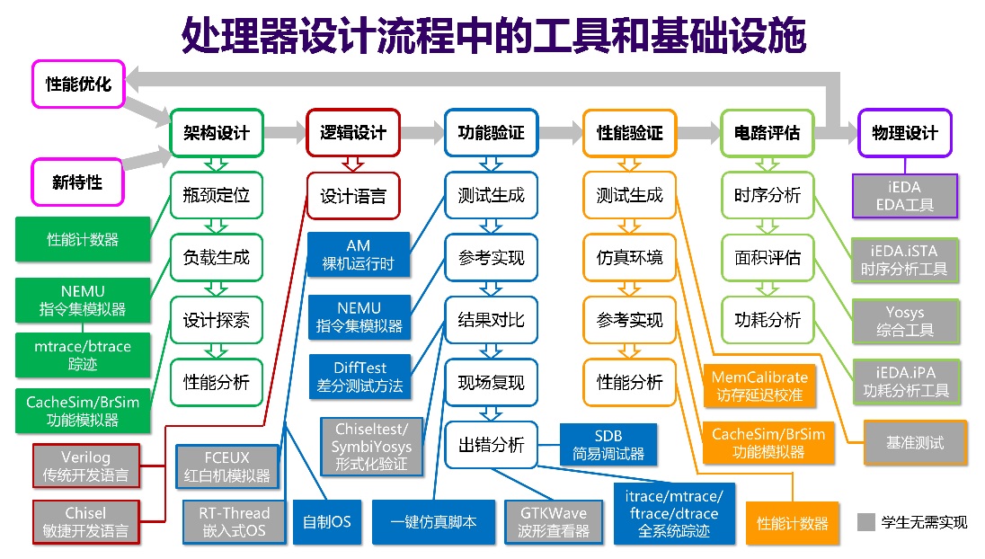
Besides the steps mentioned above, the modern processor design flow includes more stages, as shown in the figure below. We list some of the problems that need to be solved in the modern processor design flow:
- Architecture Design: Given a new feature (which may be functions from ISA specifications such as adding new instructions, or functional optimization schemes at the processor level), how to propose a design scheme and decompose it into appropriate hardware modules to implement it?
- Logic Design: With a design scheme in place, how to implement the hardware modules in the scheme at the circuit level through HDL?
- Functional Verification: How to verify that the circuit described by HDL meets the expected functions of the new feature?
- Performance Verification: How to ensure that the processor's performance meets expectations?
- Circuit Evaluation: How to evaluate and optimize indicators such as the processor's frequency, area, and power consumption?
- Physical Design: How to convert HDL code into a layout that is ready for tape-out?
- Performance Optimization: How to identify and locate performance bottlenecks in the processor, and design corresponding optimization schemes?
Meanwhile, you should also realize that even the Logisim-based design process mentioned earlier still involves numerous steps you may not yet be familiar with, such as:
- How is the RISC-V instruction sequence generated from C code?
- How can a C program be developed to display the "One Student One Chip" logo on the screen?
- How to create more programs to run on the processor?
Processor Design ≠ HDL Coding
Many students in electronics-related majors may simplistically equate processor design with "HDL coding." This view is one-sided: as illustrated in the diagram above, HDL coding only accounts for the logic design phase, while the entire design flow encompasses far more stages. In reality, numerous aspects of processor design are intimately linked to software, for the following reasons:
- Processors depend on software to function: A processor operates by executing instructions, and these instructions are software. To evaluate a processor, we assess whether software runs correctly and efficiently on it.
- The design flow relies on software tools and infrastructure: Each step in the process (e.g., instruction-set simulators, functional simulators, differential testing methods) requires supporting tools, which are essentially software and critical to advancing the design.
- HDL code itself is a form of software: While HDL describes hardware, as code, it demands software engineering practices for management, maintenance, testing, and optimization. As the codebase scales, these issues grow increasingly important—fortunately, software engineering has addressed such challenges for decades, so we can draw on its lessons.
In short, designing a capable processor requires recognizing the vital role of software.
You may not fully understand these concepts now, and we won’t delve into them here. Going forward, we’ll abandon Logisim and gradually build a modern processor design flow. Your understanding of these questions will naturally clarify as we progress.
Are you ready to step into the world of code-driven hardware design?