F3 The basic of digital and logic circuits
Don't use night mode to read this chapter.
In night mode, the image display will be difficult to recognize, it is recommended to use day mode for reading.
Processor chips are essentially digital circuits. Therefore, to learn processor chip design, knowledge of digital circuits is fundamental. Digital circuits are circuits used to process digital signals, simply which are discrete signals consisting of 0 and 1. The 0 and 1 here are not natural numbers in the mathematical sense,they refer to two different states of a signal. Physically, these correspond to the signal's Potential states, typically low and high levels. For simplicity, we will refer to them as 0 and 1, respectively. The 0 and 1 here are not natural numbers in the mathematical sense,they refer to two different states of a signal. Physically, these correspond to the signal's Potential states, typically low and high levels. For simplicity, we will refer to them as 0 and 1, respectively. To distinguish them from the mathematical 0 and 1, these two states are sometimes referred to as logical 0 and logical 1. Analog signals are the opposite of digital signals. Analog signals are usually continuous, such as current and voltage. Circuits that process analog signals are called analog circuits, but we rarely pay attention to them in processor design.
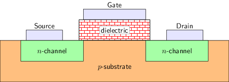
Realizing 0 and 1 through transistors In digital circuits, 0 and 1 are implemented using transistors. The most commonly used transistor is the Metal-Oxide-Semiconductor Field-Effect Transistor (MOSFET), abbreviated as MOS transistor. Based on their operating principles, MOSFETs are further classified into two types: nMOS (N-type MOS, where N stands for Negative) and pMOS (P-type MOS, where P stands for Positive). Both types have three terminals: the gate, source, and drain. Their side views are shown in the figure below.
 |  |
|---|
Transistors are typically used as circuit components and are connected to circuits like switches. However, unlike manually operated switches, transistors are special switches that are controlled by the voltage in the circuit.
Taking nMOS as an example, according to its electrical characteristics, the functionality of nMOS is as follows:
- When the difference between the gate voltage and the source voltage () is large, the source and drain are conductive, equivalent to the switch being closed
- When the difference between the gate voltage and the source voltage () is small, the source and drain are cutoff, equivalent to a switch being open.
The functionality of a pMOS is similar to that of an nMOS: it conducts when is large and is cutoff when is small.
How exactly do transistors control switches through voltage?
Understanding this issue requires some knowledge of physics and chemistry, but this is beyond the scope of processor design. Therefore, it is not essential knowledge for the "One Student One Chip(OSOC)" learning process. If you are truly interested in this issue, we can provide a brief explanation. Taking nMOS as an example, when manufacturing nMOS, a small amount of specific impurity elements are doped into a silicon material to form a P-type substrate (the p-substrate in the figure above),these impurity elements are unstable and easily lose an electron, allowing electrons to move freely within the P-type substrate.
Then, two N-regions (the n-channel in the figure above) are etched into the substrate, and a large amount of another type of impurity element is doped into them, followed by the use of metal to connect two electrodes, serving as the source and drain, respectively.A layer of silicon dioxide is then deposited on the substrate surface as an insulating layer (as shown in the dielectric layer in the figure above), and metal electrodes are used as gate electrodes on top of the insulating layer.
When working, applying a sufficiently high voltage to the gate creates an electric field beneath the insulator.Under the influence of the electric field, the free-moving electrons in the P-type substrate will move toward the insulator. However, since electrons cannot pass through the insulator, they will accumulate beneath it, forming a conductive channel. This channel connects the source and drain of the N-region, and the nMOS is in the conductive state.Conversely, if the voltage applied to the gate is insufficient, the channel cannot form, and the source and drain cannot be connected, at which point the nMOS is in the cutoff state. The operating principle of the pMOS is similar to that of the nMOS but not entirely the same.Interested students can search for related materials
Since NMOS and PMOS have complementary characteristics, they are typically used together in digital circuits,referred to as CMOS (Complementary Metal-Oxide-Semiconductor) technology.
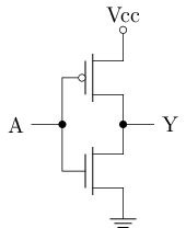
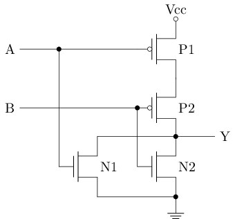
This is a very simple CMOS circuit:
 |  |  |
|---|
This CMOS circuit works as follows:
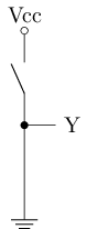
When a high voltage is applied at point A, the n-channel transistor (nMOS) below conducts, and the p-channel transistor (pMOS) above cuts off, which is equivalent to point Y being connected to ground (middle picture), and the voltage at point Y is low.
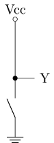
When a low voltage is applied at point A, the n-channel transistor (nMOS) below is turned off, and the p-channel transistor (pMOS) above is turned on, which is equivalent to point Y being connected to the power supply (right picture), and the voltage at point Y is high.
We can see that CMOS circuits convert the switching characteristics of n-type and p-type transistors into high or low circuit output voltages
Defining a high physical voltage (such as ) as logical 1 (high level) and a low voltage (such as ) as logical 0 (low level), we obtain the two basic states of signals in digital circuits!
Building logic gates with transistors Representing 0 and 1 is not enough,we also need to use CMOS circuits to perform various meaningful conversions on 0 and 1. This process is called digital signal processing.
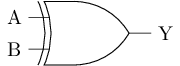
Not gate(Inverter)
Considering the CMOS circuit described above, when the input at point A is 1, the output at point Y is 0; when the input at point A is 0, the output at point Y is 1. This is exactly the logical NOT operation! This gate circuit is a NOT gate, also known as an inverter.
 |
|---|
NAND gate
Let's look at another gate circuit.
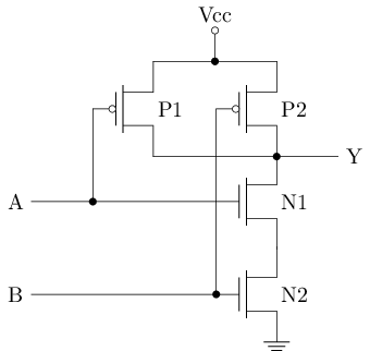 |  |
|---|
It is difficult to understand the function by looking at the structure directly, so we need to sort out its behavior. Specifically, since P1 and P2 are connected in parallel, when one of them is conductive, Y is 1; In addition, since N1 and N2 are connected in series, when both are conductive, Y is 0. Therefore, we can organize the following table:
| A | B | P1 | P2 | N1 | N2 | Y |
|---|---|---|---|---|---|---|
| 0 | 0 | conductivity | conductivity | cut-off | cut-off | 1 |
| 0 | 1 | conductivity | cut-off | cut-off | conductivity | 1 |
| 1 | 0 | cut-off | conductivity | conductivity | cut-off | 1 |
| 1 | 1 | cut-off | cut-off | conductivity | conductivity | 0 |
According to the table above, when both inputs are 1, the circuit output is 0, otherwise the output is 1. This is exactly the logical NAND operation! This gate circuit is a NAND gate.
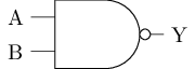
AND gate
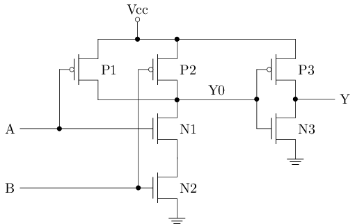
Connecting the output of a NAND gate to the input of a NOT gate results in an AND gate. Compared to a NAND gate, the output terminal of an AND gate's logic symbol has one less circle. In the logic symbol of a gate circuit, this circle represents inversion.
 |  |
|---|
Analyzing gate circuits
Try to analyze the behavior and function of the following gate circuit.
 |
|---|
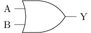
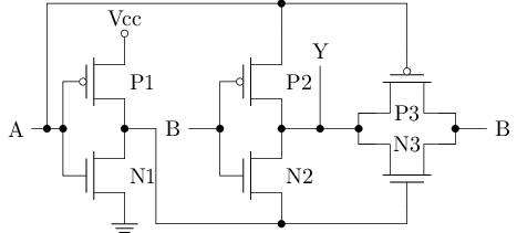
Or gate transistor structure
The following is the logical symbol for an OR gate. Try to draw the transistor structure of an OR gate.
 |
|---|
Three-input NAND gate
The gate circuits described above all have two inputs. Sometimes it is necessary to perform operations on multiple input signals. One example is a three-input NAND gate. If we express its behavior using a logical expression, we have Y = ~(A & B & C), where & represents the AND operation.
Based on this logical expression, we can build a three-input NAND gate using a two-input AND gate and a two-input NAND gate (left picture). Another way is to use transistors to build a three-input NAND gate (right picture).
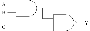 | 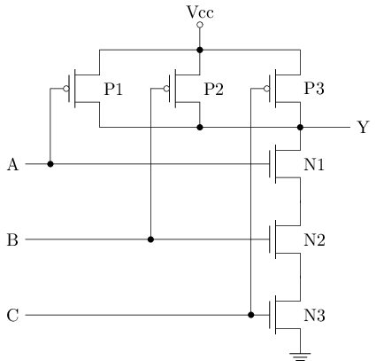 |
|---|
Comparison of the number of transistors required for the two implementations
It is not difficult to analyze that the above transistor structure also realize the function of a three-input NAND gate.Try to compare the number of transistors required in the two implementations.
Hint: For designs built with gate circuits, The number of transistors can be considered as the sum of the number of transistors used in all gate circuits in the design.
Fully customized circuitry: Circuitry designed using transistors
Circuits designed at the transistor level are called fully customized circuits. Through the example of a three-input NAND gate, we can see that fully customized circuits require fewer transistors and therefore have a smaller circuit area. In actual production, in addition to having a smaller area, fully customized circuits also have a higher main frequency and lower power consumption.
However, designing fully customized circuits is difficult and the development cycle is long.
Modern processor chips contain hundreds of millions of transistors, and it is impractical to develop them all using fully customized circuits. For the design of very large-scale integrated circuits, it is more common to use a semi-custom circuit design method.
The design of semi-custom circuits can be further divided into two methods: the standard cell-based design method and the gate array-based design method.
The former involves pre-designing some commonly used logic units, such as AND gates, OR gates, and flip-flops, using a fully custom approach.
These logic units are referred to as standard cells.Then, large-scale circuits are constructed using these standard cells. Returning to the example of the three-input NAND gate, if the two-input AND gate and the two-input NAND gate are considered standard cells, then to construct the three-input NAND gate using them can be regarded as a semi-custom circuit design method.
As for design methods based on gate arrays, a common example is FPGA.
However, we don't plan to use FPGA in the future. Interested students can search for relevant information.
In modern processor chip design, semi-custom circuit design methods based on standard cells are used in most cases.
Only when pursuing ultimate performance (e.g. when a company's products dominate the market by pursuing high performance) will some of the core modules in the circuit be fully customized.
XOR gate
An XOR gate is used to perform exclusive OR (XOR) operations. Its logic symbol is shown in the figure below.
 |
|---|
XOR is a special calculation typically used when processing logical data. Its truth table is as follows:
| A | B | Y |
|---|---|---|
| 0 | 0 | 0 |
| 0 | 1 | 1 |
| 1 | 0 | 1 |
| 1 | 1 | 0 |
There are two ways to understand the behavior of the XOR operation:
The "X" in XOR stands for "different," so when inputs A and B are different, the result is
1,otherwise, it is0.The OR operation indicates that at least one of the two inputs is
1. Unlike the AND operation, the XOR operation excludes the case where both inputs are1, so it is also called "exclusive OR," where ‘exclusive’ corresponds to the English term "exclusive",Conversely, the OR operation is also called "compatible OR," indicating that both inputs can be1.
With the truth table, we can obtain the corresponding logical expression. The corresponding steps are as follows:
- Describe a table entry based on the input conditions. For each table entry in the truth table, consider each input signal. If the input is
1, take the input signal itself; if the input is0, take the negation of the input signal. Perform a bitwise AND operation on these signals to obtain the description of the table entry. For example, the description corresponding toA = 1, B = 0in the table isA & ~B. - Combine the corresponding descriptions of table entries with an output of
1into the final logical expression.
Consider the table entries where the output is 1 in the truth table. Perform a logical OR operation on the descriptions of these table entries. For example, in the truth table for the XOR operation, there are two cases where the output is 1: One is A = 1, B = 0, corresponding to the description A & ~B; the other is A = 0, B = 1, corresponding to the description ~A & B. Performing a logical OR operation on these two descriptions yields the logical expression for the XOR operation: Y = A ^ B = (A & ~B) | (~A & B).
Unlike the AND operation, the XOR operation excludes the case where both inputs are 1, so it is also called "exclusive OR," where ‘exclusive’ corresponds to the English term "exclusive"; Conversely, the OR operation is also called "compatible OR," indicating that both inputs can be 1.
With the truth table, we can derive the corresponding logical expression, following these steps:
- Describe a table entry based on the input conditions. For each table entry in the truth table, consider each input signal: if the input is
1, take the input signal itself; If the input is0, take the negation of the input signal. Perform a AND operation on these signals to obtain the description of the table entry. For example, the corresponding description forA = 1, B = 0in the table isA & ~B. - Combine the corresponding descriptions of the table entries with an output of
1to form the final logical expression. Consider the table entries with an output of1in the truth table, and perform a logical OR operation on the descriptions of these entries. For example, in the truth table for the XOR operation, there are two cases where the output is1: one isA = 1, B = 0, with the corresponding description beingA & ~B; the other isA = 0, B = 1, corresponding to the description~A & B. Performing a logical OR operation on these two descriptions yields the logical expression for the XOR operation:Y = A ^ B = (A & ~B) | (~A & B).
The above steps can always convert a truth table into a logical expression composed of AND and OR operations. Based on this logical expression, you can easily build the corresponding circuit using AND gates and OR gates.
Karnaugh Map Simplification
You may have heard of this technique in some digital circuit textbooks;if you haven't, that's fine. You may need to learn it for exams, but in hands-on projects such as "One Student One Chip," you won't ever use it.
What we express is that this technology has very low scalability: In real-world projects, the number of variables you encounter is likely to be five or more, and could even reach as high as a dozen or more. Using a Karnaugh map to simplify expressions is highly inefficient. In fact, modern tools typically use the QMC algorithm or the Espresso algorithm to simplify logical expressions, Therefore, you rarely need to manually simplify logical expressions, The methods described above are sufficient to help you write a correct logical expression; the simplification work can be given to modern tools. If you are interested in it, you can search for related information to learn more about these algorithms.
Build an XOR gate using other logic gates.
Try to build an XOR gate in Logisim using the gate circuits mentioned above. After building up, using simulation to check whether your plan is correct.
You have verified that your solution is correct, to calculate how many transistors your solution uses.
Looking for a better construction plan
Without considering fully customized circuits, try to find a solution with the fewest transistors to implement an XOR gate and test your solution in Logisim to see if it is correct.
Hint:There is a solution that requires only 14 transistors, so the optimal solution should use no more than 14 transistors.
Fully customized circuit for XOR gates
The picture below shows a fully customized implementation of an XOR gate. Try to analyze its behavior.
 |
|---|
Design XNOR gate
There is another operation called the "XNOR" operation. When inputs A and B are the same, the result is 1; otherwise, it is 0. The XNOR operation can be considered the inverse of the result of the XOR operation.
Try to build an XNOR gate in Logisim using the gate circuits mentioned above. After building it, use the simulation to check if your design is correct.
Fully customized circuit for XNOR gates
Try to build a XNOR gate using the minimum number of transistors.
Hint:There is a solution that only requires six transistors, so the optimal solution should use no more than six transistors.
Machine representation of integers
We already know that CMOS circuits can represent and deal with 0 and 1.
However, the physical world we live in is not limited to 0 and 1. Therefore, we need to consider how to use 0 and 1 to represent various types of information in the physical world. This representation method is called "encoding." There is a lot of information in the physical world. Let's first consider how to represent integers.
Binary encoding of integers
We already have a basic understanding of the concept of "numbers" in secondary school and even kindergarten.
In daily life, we use the decimal counting system. The true value of a decimal number (i.e., the actual value it represents) can be obtained through a weighted sum expansion.
For example, the weighted expansion of the decimal number 734 is as follows:
For an -digit base- number , its true value can be obtained through the following weighted sum expansion formula:
Among them, is called the base, and is called the weight of each digit.
Let , and let take values only from 0 and 1, and we obtain the binary counting method.
Since the decimal system also uses 0 and 1, it is generally necessary to add some prefixes or subscripts in writing to indicate that a number is represented in binary: Some programming languages use the prefix 0b to denote binary numbers, such as 0b00101110;
Some textbooks use the subscript B to denote binary numbers, such as . In this lecture notes, we mainly use the prefix 0b. For example, the truth value of the binary number 0b00101110 is
To convert a binary number to a decimal number, you can use the following weighted sum expansion formula to obtain decimal number:
To convert a decimal number to a binary number, we need to find the weighted sum expansion of each binary digit . To do this, we can rewrite the above weighted sum expansion as follows:
Through the above rewriting, we can see that if we continuously divide a decimal number by 2, the remainders obtained in this process correspond to . We can use "short division" to list this calculation process. For example, for the decimal number 46:
2 | 46   -> 0          ^  lower-bit
  +----                |
 2 | 23   -> 1         |
   +----               |
  2 | 11   -> 1        |
    +----              |
   2 | 5    -> 1       |
     +----             |
    2 | 2    -> 0      |
      +----            |
     2 | 1    -> 1     |  higher-bit
       +----
         0 (Business is zero, end.)
Finally, combining the remainders from high to low to obtain 0b101110, which is the binary representation of 46. Consistent with the aforementioned 0b00101110 after omitting the high-bit 0.
Hexadecimal encoding of integers
Although binary can be processed directly by digital circuits, it is difficult for people to read and remember.
For example, for the binary number 0b1011111011101111, it is hard to tell at a glance how many bits it has.
In addition, converting between binary and decimal numbers requires certain mathematical calculations,which are usually not to finish quickly. In order to solve these problems,the computer domain also usually uses the hexadecimal counting system.
In the hexadecimal number method, each digit has 16 possible values, in addition to 0~9, there are also a, b, c, d, e, f (uppercase is also acceptable),which represent the values 10, 11, 12, 13, 14, 15, respectively.
Some programming languages use the prefix 0x to represent hexadecimal numbers, such as 0xbeef; Some textbooks use the subscript H to represent hexadecimal numbers, such as .
In this lecture note, we mainly use the prefix 0x. Similarly, conversions between decimal and hexadecimal can be performed using weighted sum expansion and short division.
For example, the weighted expansion of the hexadecimal number 0xbeef is as follows:
Although digital circuits cannot directly process hexadecimal numbers, since ,it is possible to convert between 1-bit hexadecimal numbers and 4-bit binary numbers,which greatly improves the efficiency of conversion between hexadecimal and binary.
For example, for the binary number 0b1011111011101111, we can group every 4 bits from right to left (padding with 0s when the high-order bits are less than 4), and directly write out the corresponding hexadecimal digits for each group:
     1011 1110 1110 1111
      |    |    |    |
      b    e    e    f
Therefore, the hexadecimal number corresponding to this binary number is 0xbeef. You can see , compared to the binary representation 0b1011111011101111, the hexadecimal representation 0xbeef is more brief and compact.
Octal number method
In computers, octal is also used in some scenarios, and its principle is similar to that of hexadecimal. Interested students can derive the conversion methods between octal and decimal, as well as between octal and binary, on their own.
Build basic combinational logic circuits using gate circuits
With gate circuits, we can build some modules commonly used in digital circuits by combining multiple gate circuits.
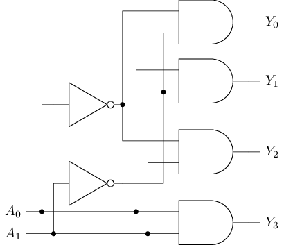
Decoder
A decoder is a circuit that converts a -bit input into to different outputs.
A common type of decoder is the 1-of-n decoder, which has bits of input and bits of output. Its behavior is as follows:
It parses the input into a binary value and sets the th bit of the output to 1, with all other bits set to 0.
Since only one bit of the output is 1, it is also called a "one-hot code."
For example, a 2-4 decoder has a 2-bit input and a 4-bit output . Its truth table and circuit diagram are as follows:
| 0 | 0 | 0 | 0 | 0 | 1 | |
| 0 | 1 | 0 | 0 | 1 | 0 | |
| 1 | 0 | 0 | 1 | 0 | 0 | |
| 1 | 1 | 1 | 0 | 0 | 0 |
 |
|---|
Build 2-4 decoders
try to build a 2-4 decoder in Logisim using gate circuits. It has 2 input bits and 4 output bits. After building it, use simulation to check if your design is correct.
Logisim also provides ready-made components such as decoders,but we still require everybody to build them using gate circuits,in order to better learn the basic principles of digital circuits.
In computers, n-to-1 decoders are often used to implement part of addressing functions. At the time, the input of the decoder is the address, and the output is the select signal, where the selection signal corresponding to the address is 1.
Configure the number and polarity of gate circuit inputs
In Logisim, users can configure the number and polarity of gate circuit inputs. The polarity attribute can be used to select whether a signal should be inverted before being sent to the logic gate. If it is, an additional circle will appear on the corresponding input terminal to indicate inversion. For specific configuration methods, please refer to the official documentation on gate circuits.
Addressing and Addressing
"Address" is a technical term in the field of computer science, but we can also understand it through examples from daily life. You have probably used Excel software to view tables. In a table, each row stores an item, and multiple items are typically stored consecutively in increasing by row number. In Excel, the row number is also displayed on the far left, allowing you to quickly determine which row you are currently viewing. If you need to view the item in row 176, you wouldn't start from row 1 and check each row to see if it's row 176, However, you can simply drag the scroll bar to quickly locate the 176th row. This is because row numbers are continuous, allowing you to quickly skip over previous rows.
In fact, many data sets in computers are also stored continuously like tables. For example, memory can be viewed as a massive table, where each row is a storage unit capable of holding 1 byte of data. stick, this table has rows. Similarly, thanks to the continuity between storage units, if a computer needs to access one of these storage units. It doesn't need to check sequentially starting from the first storage unit,instead, it can quickly locate the corresponding storage unit using a "row number." This "row number" is referred to as an ‘address’ in a computer, and the process of locating the corresponding storage unit based on the address is called "addressing."
The reason why computers can quickly find the corresponding storage unit through addresses is that computers can quickly convert addresses into a set of selection signals through n-to-1 decoders, and then select the target data through this group of selection signals.
Subcircuit Function in Logisim
Decoders are frequently used in subsequent digital circuit designs. To avoid users having to redesign the same circuit repeatedly, Logisim provides a subcircuit function, allowing the corresponding circuit to be designed once and then instantiated repeatedly in subsequent designs. For specific instructions, please refer to the "Subcircuits" section of the official manual.
After learning how to use Logisim's subcircuit function, try to encapsulate the decoder you designed into a subcircuit.
Decoder extension
The 3-8 decoder has 3 input and 8 output. Try to instantiate two 2-4 decoders and add a few logic gates to implement the functionality of the 3-8 decoder. After building, using simulation to verify that your design is correct.
In Logisim, the input signals and output signals are typically connected to input or output components, and the current values of the input signals or output signals can be determined by the state of these components. If you want to know the current value of middle signals, you can use the Probe component provided in the component library. You can find it in the Wiring category of the Logisim component library. For specific use instructions, please find the friendly mannual.
Data width of configuration components
In Logisim, users can configure the data bit width of components. For example, when the data bit width of an AND gate is set to 4, it means that each port can connect to 4-bit signals. At this time, it is functionally equivalent to using 4 1-bit AND gates to process each bit of the 4-bit signal separately. With the data bit width function, users can easily design circuits with similar processing modes. For specific configuration methods, please refer to the official documentation on gate circuits.
Additionally, you may need to extract several bits from a group of signals or combine several bits of signals into a single group for overall connection,which requires the use of a Splitter. You can find it in the Wiring category of the Logisim component library. For specific usage instructions, please find the friendly mannual.(RTFM)
Another common type of decoder is a code translator,which can convert an input encoded in one format into an output encoded in another format according to specified rules. Unlike an n-to-1 decoder, a code translator doesn't require the output to contain at most one 1.
A common application of a code translator is a 7-segment decoder.
A 7-segment tube display is an output device composed of seven segments of light-emitting diodes arranged in an "8" shape, as shown in the photo below.
The letters a-g are used to identify the position of each segment of light-emitting diodes. As long as a control signal is active, the corresponding light-emitting diode will be lit up. There is also a decimal point marked with the letter h, which is used in some scenarios that require decimals.
   a
  ---
f| g |b
  ---
e|   |c
  ---    .h
   d
The function of a seven-segment tube display decoder is to parse a set of four-digit input signals into binary integers,then output a set of control signals used to Control signal for controlling the lighting and extinguishing of seven-segment digital tubes,so that the seven-segment digital tube can display and input the corresponding numbers.
For example:
input    output
        abcdefgh
 0100   01100110
The above example demonstrates how to display the number 4 on a seven-segment display to show.
Specifically, to display the number 4, the b, c, f, and g segments of the seven-segment display must be illuminated,so the corresponding control signals must be set to active (here assuming high-level active; in actual use, verify the input polarity of the seven-segment tube display component);
For other diodes that don't need to be illuminated, the corresponding control signals must be set to inactive.
If arrange from left to right as a-h, the output control signal should be 01100110. Since 4 corresponds to the binary representation 0b0100, the seven-segment display decoder must output 01100110 when the input is 0100. Using the same method, You can analyzed the input and output conditions for each digit from 0 to 9.
Build a seven-segment digital tube decoder
Try to build seven-segment display decoder using logic gates in Logisim. It has 4 input and 8 output,connected to a DIP switch and a seven-segment digital tube display, respectively. The seven-segment display decoder supports the display of decimal numbers, meaning that when the input corresponds to 0-9, he seven-segment display shows the corresponding number; for other inputs, the seven-segment digital tube display only shows the decimal point. After building, using simulation to check if your implementation is correct.
Hint:
- seven-segment display components can be found in the component library. After instantiation,you can hover the mouse pointer over the component's port to view the port's functional description.
- You can first use an N-to-1 decoder to generate a group of unique codes,then use a layer of AND gates to determine which inputs should cause each LED to light up.
Build seven-segment display decoder (2)
Try to build a seven-segment display decoder that supports hexadecimal numbers through using gate circuits in Logisim. Compared to the decimal numbers mentioned above, when the input corresponds to 10-15,the seven-segment display display shows A, b, C, d, E, and F, respectively. After building it, using simulation to check if your implementation is correct.
Encoder
The function of an encoder is the opposite of that of an n-to-1 decoder; it is used to convert a unique code into the corresponding binary value. Specifically, an encoder has input bits and output bits. If the input is a One-hot code and the th bit is 1, then the output is the binary value of .
If the input is not a One-hot code, the output is undefined.
For example, a 4-2 encoder has 4-bit input and 2-bit output , with the following truth table. In the table below, when the input isn't a One-hot code, the output is X, indicating that the output is undefined and can be any value.
| 0 | 0 | 0 | 1 | 0 | 0 | |
| 0 | 0 | 1 | 0 | 0 | 1 | |
| 0 | 1 | 0 | 0 | 1 | 0 | |
| 1 | 0 | 0 | 0 | 1 | 1 |
Understanding undefined output
Some calculations or modules require certain precondition to be met in order to produce meaningful output. One example is the mathematical calculation of division. You may have heard something like this: "You can't divide by 0." The phrase "can't divide" here is natural language, not the language of the mathematical system. If using mathematical language to descibe it, "the divisor is not 0" is a precondition for performing division. When the divisor is 0, this precondition no longer holds, and it is impossible to define a correct and meaningful calculation result. Therefore, the result is also referred to as undefined.
The example of the encoder is similar. "The input is a One-hot code" is a precondition for the encoder to operate correctly. When the input is not a One-hot code, this precondition no longer holds, and it is impossible to define a correct and meaningful output.
However, at the digital circuit level, the output signal is either 0 or 1,but regardless of the value taken, the meaning of the output signal is incorrect. But since that's the case, the circuit designer can assign any value to the output signal under these undefined conditions.
There is actually an agreement behind this design method: If the encoder user wants the encoder to output correct results, they must ensure that the precondition of "input being One-hot code" is met; Conversely, if this precondition is not met, then the encoder user is violating the convention, and the encoder's output is meaningless. If subsequent circuits process these meaningless outputs, the resulting consequences are the responsibility of the encoder user.
Therefore, when designing an encoder, we can ignore the outputs in other cases, and only need to ensure that the correct output is obtained when the input is One-hot code: , .
Build encoder
Try to build a 16-4 encoder in Logisim using gate circuits. It has 16-bit input and 4-bit output,connected to a DIP switch and a seven-segment display decoder,so that the encoder's output results are displayed as hexadecimal numbers on the seven-segment display. After building it, using simulation to check if your implementation is correct.
In computers, encoders are commonly used to generate corresponding addresses based on selection signals represented by unique codes. Another interpretation is that they are used to determine the position of 1 in One-hot code.
The above encoder requires the user to ensure that the input is One-hot code. If you wish to output valid information even when the input is not One-hot code,you need to use another type of encoder —— priority encoder.
A priority encoder has input bits and output bits. Unlike the encoders described above, a priority encoder allows multiple 1s in the input signal.
In this case, the highest-bit 1 is prioritized in the encoding. Therefore, if the input is not all zeros, the output is the position of the highest-bit 1; if the input is all zeros, the output is undefined.
For example, a 4-2 priority encoder has 4-bit input and 2-bit output , with the following truth table.
| 0 | 0 | 0 | 1 | 0 | 0 | |
| 0 | 0 | 1 | X | 0 | 1 | |
| 0 | 1 | X | X | 1 | 0 | |
| 1 | X | X | X | 1 | 1 | |
| 0 | 0 | 0 | 0 | X | X |
Build the 4-2 priority encoder
Based on the truth table above, try to list the logical expressions for each output bit. Then try to build a 4-2 priority encoder in Logisim using gate circuits. After building it, simulate it to check if your solution is correct.
After implementation, compare the number of gate circuits required for the 4-2 encoder and the 4-2 priority encoder.
Extension of the priority encoder
The 16-4 priority encoder has 16-bit input and 4-bit output. Try to instantiate several 4-2 priority encoders and add a few logic gates to achieve the functionality of a 16-4 priority encoder. Then connect the 16-4 priority encoder to a DIP switch and a seven-segment display decoder, so that the output results are displayed as hexadecimal numbers on the seven-segment display. After building it, using simulation to check whether your implementation is correct.
Counting of leading 0 and leading 1
Sometimes, a computer needs to calculate the number of "leading zeros" in a piece of data, that is, the number of consecutive 0 in the high-bit bits of the binary representation of the data. Assuming the data width is 16 bits, for the data 16392, its binary representation is 0b0100000000001000, so the number of leading zeros is 1.
Similarly, we can define "trailing 0", which refers to the number of consecutive 0 in the lower bits of the binary representation of the data. Using the data 16392 as an example, the number of trailing 0 is 3. Similarly, we can define "leading 1" and "trailing 1."
Think about how to quickly calculate these using a priority encoder?
Multiplexer
The Multiplexer can select one of the multiple data terminals for output according to the input of the control terminal. A multiplexer is also known as a "multiplexer" or simply a "selector." The simplest selector is a "1-bit 2-to-1 selector," which can choose one of the two 1-bit data for output according to the input of the control terminal. The logic symbol, circuit structure, and truth table for a 1-bit 2-to-1 selector are as follows:
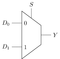 | 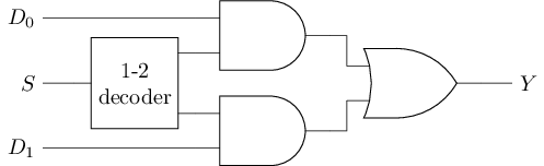 |
|---|
| 0 | ||
| 1 |
As we can see, the selector contains an n-to-1 decoder. If the control signal of the selector is regarded as an address, this n-to-1 decoder generates the corresponding selection signal. This group of selection signals allows the selected data to successfully pass through the AND gate, while the unselected data will become 0 after passing through the AND gate. Finally, the selected data is transmitted to the output end through an OR gate.
Build a 1 bit 2-to-1 selector
Try to build a 1-bit 2-to-1 selector in Logisim using gate circuits. After building it, using simulation to check if your design is correct.
In computers, selectors are frequently used components,because computers are essentially used to process data, and there are many sources and processing methods for data. Therefore, a large number of selectors are needed to select data sources and processing results.
Build a 3-bit 4-to-1 selector
Then build a 3-bit 4-to-1 selector in Logisim using logic gates. After building it, use simulation to verify that your design is correct.
- If you do not understand the meaning of a "3-bit 4-to-1 selector," you should first carefully read the explanation of the "1-bit 2-to-1 selector" in the preceding text.
- For each bit in the data, you can reuse the selection signals generated by the n-to-1 decoder for selection.
Build a seven-segment display with switchable carry counting system
Using 5 DIP switches and 1 seven-segment display, the following functions are implemented: Among them, 4 DIP switches are used as data input, and the remaining 1 DIP switch is used as the choice of carry counting system. When the selection signal is 0, the seven-segment display shows the data in decimal format; When the selection signal is 1, the seven-segment display shows the data in hexadecimal format. When the input data is 10-15, the two display way differ.
Comparator
Comparators are used to check whether each bit of two inputs is completely consistent. Since XOR gates (and XOR gates) already have the function of comparing 1-bit data,so multiple-bit data comparators can be built using XOR gates (and XOR gates). The following picture shows the circuit structure of a 4-bit comparator:
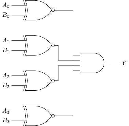 |
|---|
Build comparator
Try to build a 4-bit comparator in Logisim using gate circuits, then use two groups of DIP switches to compare whether the two groups of data are equal. Try to build a 4-bit comparator in Logisim using gate circuits, then use two groups of DIP switches to compare whether the two groups of data are equal. If they are equal, lighting up an LED. After building it, using simulation to check whether your solution is correct.
Adder
Addition is the foundation of arithmetic calculations, so it is necessary to consider how to implement addition using logic gates.
First, We can consider a 1-bit adder. The inputs to addition are two addends, and the outputs are the sum S;
The result of addition may generate a carry, so to avoid losing this information, the carry C must also be output. Based on the rules of addition, we can easily list the truth table for a 1-bit adder:
A | B | S | C | |
|---|---|---|---|---|
| 0 | 0 | 0 | 0 | |
| 0 | 1 | 1 | 0 | |
| 1 | 0 | 1 | 0 | |
| 1 | 1 | 0 | 1 |
S = A ^ B, C = A & B. Specifically, the sum is 1 if and only if the two addends are different; the carry is 1 if and only if both addends are 1. Based on the truth table, we can obtain the logical expressions for S and C: S = A ^ B, C = A & B.
When considering a multi-digit adder, since the carry generated by the lower bit needs to be incorporated into the addition process of the higher bit,we need to design a new adder that can use the carry propagated from the lower bit as input:Specifically, this adder has three inputs A, B, and Cin, where Cin represents the carry propagated from the lower bit; it has two outputs S and Cout, where Cout represents the carry output generated by the addition operation. To distinguish it from the adder described above, this type of adder with carry input is called a full adder (FA), while the adder without carry input described above is called a half adder (HA).
Build a full adder
Try to list the truth table for a 1-bit full adder and build a 1-bit full adder in Logisim using gate circuits. After building it, using simulation if your solution is correct through simulation.
Build a full adder (2)
Try to instantiate several half-adder circuits and adding a few logic gates to implement a 1-bit full adder. After building it, using simulation if your solution is correct through simulation.
With a full adder, we can use it to build a multi-bit adder. For example, the picture below shows the circuit structure of a 4-digit adder. As we can see, the working principle of a multi-bit adder is similar to the calculation process of multi-bit addition learned in elementary school, They are both involving step-by-step calculation from the least significant bit to the most significant bit. However, while elementary school teaches decimal addition, here we are discussing binary addition. This type of multi-bit adder is called a "Ripple-Carry Adder" (RCA), because the carry generated during the calculation process propagates from the lower bit to the higher bit like a wave.
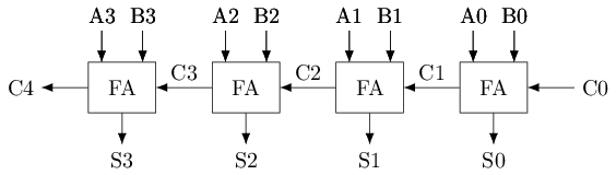 |
|---|
Build a 4-bit adder
Try to build a 4-bit adder in Logisim using gate circuits. Use a seven-segment display to show the two inputs and the result of the adder in hexadecimal. Use an LED to show if there's a carry in the addition result. After building it, using simulation if your solution is correct.
Encoding of integers
Review the examples mentioned in the binary representation described above.
In this representation, each binary bit represents the magnitude of the true value. This representation is called an "unsigned binary integer," simply called "unsigned number." Obviously, in an -bit unsigned number, the smallest number is , and the largest number is . The adder you just implemented is also actually an adder for unsigned numbers.
So, how should computers represent negative numbers?
In mathematics, we represent a negative number by adding a negative sign - followed by the absolute value of the negative number, such as -5.
Since computers can only process binary numbers, we need to consider how to encode integers, including negative numbers, using binary numbers. One straightforward idea is to use a single binary bit to encode the sign bit of the integer, with the remaining binary bits used to encode the absolute value of the integer.
sign-and-magnitude
The sign-and-magnitude is an intuitive encoding method, where the hignest bit represents the sign bit, 0 represents a positive number, 1 represents a negative number,and the remaining bits represent the absolute value of the corresponding truth value. For example:
0b00000111 = 7
0b10000111 = -7
0b00100010 = 34
0b10100010 = -34
Consider using 8-bit RCA for sign-and-magnitude addition:
 0b00000111 (7)     0b10000111 (-7)     0b10000111 (-7)    0b00000111 (7)
+0b00100010 (34)   +0b10100010 (-34)   +0b00100010 (34)   +0b10000111 (-7)
-----------        -----------         -----------        -----------
 0b00101001 (41)    0b00101001 (41)     0b10101001 (-41)   0b10001110 (-14)
Based on the above observations, we can draw the following conclusions:
When both numbers are positive, the result obtained by performing addition using RCA is interpreted in its sign-and-magnitude,and is mathematically equivalent to the result obtained by adding the two numbers after interpreting them in their sign-and-magnitude. Therefore, in this case, sign-and-magnitude addition can be performed directly using RCA.
When both numbers are negative, the result obtained by RCA does not align with mathematical meaning, with the difference lying in the sign bit. Therefore, in this case, the circuit must perform special handling on the sign bit.
When only one number is negative, the result obtained by RCA doesn't align with mathematical meaning,not only may the sign bit be incorrect, but the absolute value is also incorrect. Therefore, in this case, RCA can't be used for sign-and-magnitude addition.
In fact, when calculating the third case in a mathematically meaningful way, the larger absolute value should subtract the other and the sign should be taken from the larger absolute value. This means that, to perform sign-and-magnitude addition, the circuit also needs to design a subtractor and then select the correct result based on the signs and absolute values of the two numbers.
Build a 4-bit subtractor
Based on the design idea of a 4-bit adder, try to build a 4-bit subtractor in Logisim using gate circuits. Use a seven-segment display to show the two inputs and the result of the subtractor in hexadecimal. Use an LED to indicate whether the subtraction result produces a borrow. After building it, using simulation to check if your solution is correct.
Build a 4-bit sign-magnitude adder
After understanding how a sign-and-magnitude adder works, try to exploit adders, subtractors, and multiplexers to build a 4-bit sign-and-magnitude adder in Logisim. To display the sign bit, you can instantiate an additional seven-segment display. Display a minus sign - when the result is negative, otherwise don't display anything. After building it, using simulation to check if your solution is correct.
one's complement
One's complement is another encoding method that attempts to solve the problem of negative numbers in the addition of sign-and-magnitude. Specifically, for positive numbers and 0, the representation is consistent with the sign-and-magnitude;for negative numbers, the representation is the bitwise complement of the sign-and-magnitude of the corresponding opposite number. For example:
0b00000111 = 7
0b11111000 = -7
0b00100010 = 34
0b11011101 = -34
Consider using 8-bit RCA for one's complement addition:
 0b00000111 (7)     0b11111000 (-7)     0b11111000 (-7)    0b00000111 (7)
+0b00100010 (34)   +0b11011101 (-34)   +0b00100010 (34)   +0b11111000 (-7)
-----------        -----------         -----------        -----------
 0b00101001 (41)    0b11010101 (-42)    0b00011010 (26)    0b11111111 (-0)
Based on the above observations, we can draw the following conclusions:
When both numbers are positive, the result obtained by addition using RCA is interpreted as a complement, and when the two numbers are interpreted as complements and added mathematically, the results are consistent. Therefore, in this case, complement addition can be performed directly using RCA.
When one of the numbers is negative, the result obtained via RCA doesn't align with mathematical meaning, although the sign bit is correct, the absolute value portion is incorrect.
Specifically, when adding two numbers that are opposite in sign, according to the definition of two's complement, the result is always
0b11111111. Interpreted as a two's complement, the true value of the result is-0. If it is treated as a mathematical0, then the RCA result is correct.
However, if -0 is used as input for RCA calculations, an incorrect result is obtained:
 0b00000111 (7)     0b11111000 (-7)
+0b11111111 (-0)   +0b11111111 (-0)
-----------        -----------
 0b00000110 (6)     0b11110111 (-8)
The above example shows that RCA can't be used directly to calculate complement addition. To calculate complement addition, one method is to first convert the complement to its true value equivalent sign-and-magnitude,then use the sign-and-magnitude adder to calculate the result, and finally convert the result back to its true value equivalent complement.
Build a 4-bit complement adder
Try to build a 4-bit complement adder in Logisim according to the above approach. After building it, using simulation to check whether your solution is correct.
Build a 4-bit complement adder (2)
In fact, we only need to make some minor adjustments to the results obtained from RCA to obtain the correct complement addition results. Observe the calculation of 3-bit complement codes and try to identify the patterns causing discrepancies in the complement calculation results. Then, based on this pattern, add the corresponding circuitry to the RCA, thereby constructing a 4-bit complement adder using a simpler method. After construction, verifying the correctness of your design through simulation.
two's complement
Two's complement is a commonly used integer encoding method in modern computers. It further corrects the deviation in the results when calculating the complement code. Specifically, for positive numbers and 0, the representation is consistent with the sign-and-magnitude;for negative numbers, the representation is the bitwise complement of the sign-and-magnitude of the corresponding opposite number plus 1. For example:
0b00000111 = 7
0b11111001 = -7
0b00100010 = 34
0b11011110 = -34
For an -bit two's complement, the largest number is 0b011...11, corresponding to the true value and the smallest number is 0b100...00, corresponding to the true value . In two's complement, the smallest number is a special number that can't be obtained by "inverting and adding 1" to a positive number. Taking an 8-bit two's complement as an example, the largest number 0b01111111=127, when inverted and added by 1, results in 0b10000001=-127; while the smallest number 0b10000000=-128, when inverted and incremented by 1,results in 0b01111111+1=0b10000000=-128, which is the same as itself. This is because 128 exceeds the range that 8-bit two's complement can represent.
Let's assume the two's complement representation of a positive number be , and let the two's complement representation of its opposite number be . According to the definition of two's complement, we have , where denotes the bitwise complement of . Expanding the weighted binary representations on both sides, we have
Furthermore, since is either 0 or 1, is either 1 or 0, so .
Considering the truth value of , there is
Therefore, the sign bit of the two's complement code can be expanded using as the weight to obtain its true value.
For example, using this method to expand 0b11111001 with weights, we have
Consistent with the truth of the code.
Consider using 8-bit RCA for two's complement addition:
 0b00000111 (7)     0b11111001 (-7)     0b11111001 (-7)    0b00000111 (7)
+0b00100010 (34)   +0b11011110 (-34)   +0b00100010 (34)   +0b11111001 (-7)
-----------        -----------         -----------        -----------
 0b00101001 (41)    0b11010111 (-41)    0b00011011 (27)    0b00000000 (0)
Through the above observations, we can see that when calculating two's complement addition using RCA,even if the input contains negative numbers, the result obtained by RCA still makes sense mathematically. This means that we can also use RCA to calculate two's complement subtraction. This is because, in mathematical terms, A-B=A+(-B), but we have already explained that regardless of the values of A and B, the result obtained by RCA is mathematically valid, therefore
Using RCA to calculate A+(-B) = A+(-B) in mathematical terms = A-B in mathematical terms
It is because addition and subtraction of two's complement can be calculated using an adder that two's complement is commonly used to represent integers in modern computers.
Why does calculating two's complement addition using RCA yield the correct result? Take a 4-bit binary number as an example. We arrange the binary numbers in a clockwise order:
              0000 (0)
      (-1) 1111  0001 (1)
   (-2) 1110   ^    0010 (2)
 (-3) 1101     |      0011 (3)
(-4) 1100      +       0100 (4)
 (-5) 1011            0101 (5)
   (-6) 1010        0110 (6)
      (-7) 1001  0111 (7)
              1000 (-8)
RCA performs addition at the binary layer. Adding a positive number is equivalent to moving the pointer clockwise;adding a negative number is equivalent to moving the pointer counterclockwise. To ensure that the result of addition in a particular encoding aligns with mathematical meaning,the corresponding truth values must also increase in a clockwise direction. The parentheses () in the figure above illustrate an example of two's complement. As shown,as long as the boundary between 7 and -8 is not crossed, the result of two's complement addition calculated using RCA always aligns with mathematical meaning. We will discuss cases where the boundary is crossed in the following sections.
        sign-and-magnitude                                  One's complement
              0000 (0)                             0000 (0)
      (-7) 1111  0001 (1)                  (-0) 1111  0001 (1)
   (-6) 1110   ^    0010 (2)            (-1) 1110   ^    0010 (2)
 (-5) 1101     |      0011 (3)        (-2) 1101     |      0011 (3)
(-4) 1100      +       0100 (4)      (-3) 1100      +       0100 (4)
 (-3) 1011            0101 (5)        (-4) 1011            0101 (5)
   (-2) 1010        0110 (6)            (-5) 1010        0110 (6)
      (-1) 1001  0111 (7)                  (-6) 1001  0111 (7)
              1000 (-0)                            1000 (-7)
Why are the English terms for one's complement and two's complement?
In fact, complement is a concept in counting systems, and the Chinese term for it is "complement". In this counting system, to subtract a number, you can calculate it by adding the complement of that number.
In an n-bit b-based counting system, for a given number , there are two types of complements: One is the radix complement, which in this example is b's complement, defined as ; The other is the diminished radix complement, which in this example is the b-1's complement, defined as . Both of these complements can be used to calculate the result of subtraction. Specifically, when b=2, these two complements are the two's complement and the one's complement, respectively.
If you are interested in related content, please refer to Related Wikipedia page.
overflow detection
Looking back at the previous analysis, even with two's complement, there is a boundary where the encoding is continuous but the true values are not continuous,namely the boundary between 0b0111...111 and 0b1000...000, which represent the maximum and minimum numbers, respectively. If the addition calculation crosses this boundary, the result won't correspond to the mathematical meaning. Specifically, this boundary exists because, for a given number of binary bits,the range of values it can represent is always finite, so there must be values that exceed this range. This situation where the calculation result exceeds the encoding range is called "overflow." Clearly, if an overflow occurs during the calculation, the result will definitely not align with mathematical meaning. Therefore, it is typically necessary to detect whether an overflow has occurred while performing the addition calculation.
From a mathematical perspective, an overflow in the addition result occurs either when two positive numbers are added, resulting in a negative number or when two negative numbers are added, resulting in a positive number. These two cases correspond to crossing the aforementioned discontinuous boundary from two different directions. From this perspective, we only need to consider the addition of the sign bits to check for overflow. Let's consider the input and output of the sign bit corresponding to the full adder in an -bit adder:
| overflow | ||||||
|---|---|---|---|---|---|---|
| 0 | 0 | 0 | 0 | 0 | NO | |
| 0 | 0 | 1 | 0 | 1 | YES |
Only the first two items of the truth table are listed here. Given two inputs , and the carry input ,according to the logic of the full adder, we can obtain the carry output and the sum . To determine whether an overflow has occurred based on the signs of the two addends and the sum, we only need to examine , , and . For example, the first case is equivalent to "adding two positive numbers, resulting in a positive number," so no overflow occurs; while the second case is equivalent to "adding two positive numbers, resulting in a negative number", so an overflow occurs.
Detect whether overflow occurs in two's complement addition
Complete the truth table above and try to list the logical expressions for overflow conditions. Then, add overflow detection logic to the 4-bit adder in Logisim. After adding it, checking if your solution is correct through simulation.
Sequential logic circuit
The modules introduced in the previous section share a common feature: their outputs are determined entirely by their current inputs. However, the modules described above are not sufficient to implement all circuits. For example, an electronic clock needs to implement the function "new seconds = old seconds + 1",where the current output also depends on its old value.
Therefore, we need to implement a new circuit with the following two characteristics:
(1) It can read the old state of the circuit; (2) It can update the state of the circuit. A circuit with the above characteristics is called a sequential logic circuit.
It can store states, and its output is determined by both the current input and the old state. In contrast, the circuits introduced in the previous section are called combinational logic circuits, which don't have the concept of old and new states.
Cross-pairing reverse phase
For this, let's first consider how to store and read out the state of the circuit. The simplest circuit that can store states is a cross-coupled inverters,whose circuit structure is shown in the picture below:
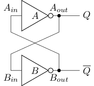 |
|---|
Assuming that is transmitted to via a network cable, and the total delay after passing through the inverter to is T,then the total delay after is transmitted to via a network cable and passes through the inverter to is also T. The behavior of the above circuit can be discussed in four cases:
- Assume that initially , i.e., . After time
T, becomes the complement of , i.e.1, while becomes the complement of , i.e.0. That is, after timeT, still holds,consistent with the state before timeT, so the circuit's state remains unchanged. - Assume that initially , i.e., . Similarly, after time
T, we still have , which is consistent with the state before timeT, so the circuit state remains unchanged. - Assume that initially , i.e., . After time
T, becomes the complement of , i.e.1, while becomes the complement of , i.e.1. That is, after timeT, we have , so the state of the circuit changes. - Assume that initially , i.e., . Similarly, after time
T, we have , so the circuit state changes.
From the above analysis, it can be seen that when or , the circuit is in a stable state that remains unchanged. We consider that the circuit can stably store 1 bit of information at this time: When , the circuit is considered to store 0; When , the circuit is considered to store 1. At this time, the state stored by the circuit can be read out through the terminal.
When or , the circuit oscillates repeatedly between these two states,with the terminal alternating between 0 and 1, unable to represent stable information. This state is called a metastable state, which may destroy other information in the circuit, causing the circuit's output to deviate from expectations. Therefore, it must be avoided during circuit design.
The following table summarizes the behavior of cross-coupled inverters:
| newQ | instruction | ||||
|---|---|---|---|---|---|
| 0 | 0 | 1 | 1 | metastability | |
| 0 | 1 | 0 | 1 | store 0 | |
| 1 | 0 | 1 | 0 | store 1 | |
| 1 | 1 | 0 | 0 | metastability |
However, even if the above cross-coupled inverter is in a stable state, we can't update its state,because this circuit has no external input, so we can't control it, making it difficult to apply in practice. To solve this problem, we need a more practical storage element.
Logisim can't build cross-coupled inverter.
Since the cross-coupled inverter has no input, Logisim can't determine its initial state. and therefore can't build a cross-coupled inverter that can be simulated. You only need to understand how a cross-coupled inverter works; you don't need to complete the related experiments.
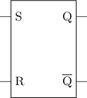
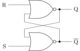
S-R latch
The SR latch provides control functions to the outside by replacing the inverters in the cross-coupled inverter with OR-NOT gates. Among them, S stands for Set, and the corresponding control terminal is used to set the latch (set to 1); R stands for Reset, and the corresponding control terminal is used to reset the latch (set to 0). The logic symbol and circuit structure of the SR latch are as follows:
 |  |
|---|
Depending on the input, we can discuss the behavior of the SR latch in four different cases:
When
S=1, R=0, the behavior of the upper OR-NOT(NOR) gate is consistent with that of the inverter, and the output of the lower OR-NOT gate is always0. At this time,Qis1, so the value stored in the SR latch is updated to1.When
S=0, R=1, the output of the upper OR-NOT(NOR) gate is always0, and the behavior of the lower OR-NOT gate is the same as that of an inverter. At this time,Qis0, so the value stored in the SR latch is updated to0.When
S=0, R=0, the behavior of the two OR-NOT(NOR) gates is consistent with that of the inverter. At this point, the behavior of the SR latch is consistent with that of the cross-paired inverter, so the SR latch will retain the previously stored value.When
S=1, R=1, the output of the two OR-NOT(NOR) gates is always0, so no valid information can be represented at this point. Additionally, when the input changes fromS=1, R=1toS=0, R=0, it is equivalent to putting the cross-coupled inverter into the state . According to the analysis above, this will cause the SR latch to enter a metastable state, so it should be avoided.
The following table summarizes the behavior of SR latches:
S | R | Q | |
|---|---|---|---|
| 0 | 0 | Keep | |
| 0 | 1 | 0 | |
| 1 | 0 | 1 | |
| 1 | 1 | Stop |
Build SR latch
Try to build an SR latch using gate circuits in Logisim. After building it, using simulation to check if your design is correct.
When operating manually, it is not possible to change two DIP switches from 11 to 00 with a single click. To trigger a metastable state, you can add several additional AND gates before the SR latch, Let another DIP switch control one of the inputs of these AND gates at the same time. This way, you can use this DIP switch to set both inputs of the SR latch to 0 at the same time. enabling you to use this DIP switch to simultaneously set both input terminals of the SR latch to 0. If you successfully trigger the metastable state, Logisim will display the message Oscillation apparent at the bottom of the window. At this point, the simulation cannot continue, and you need to reset the simulation via the Logisim menu.
SR latch constructed with NAND gates
The SR latch described above is constructed using OR-NOT(NOR) gates. In fact, the OR-NOT gates can also be replaced with AND-NOT(NAND) gates. This type of latch is called a latch. Try to list the truth table for the latch and analyze its behavior.
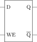
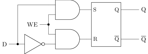
D latch
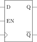
To avoid metastability at the source, we can add several gate circuits before the SR latch to limit the four inputs of the SR latch to three valid inputs. This is the basic idea behind the D latch. The logic symbol and circuit structure of the D latch are shown below, where D is the input data and WE is the write enable (Write Enable).
 |  |
|---|
Analysis of D latch behavior
Try to list the truth table based on the circuit structure diagram and analyze the behavior of the D latch.
build D latch
Try to build a D latch using gate circuits in Logisim. After building it, using simulation to check if your solution is correct.
Build a D latch with reset function
Try to add a reset input and reset function to the D latch. When the reset signal is active, the value stored in the D latch will become 0.
Implementing bit flip functionality using D latches
Instantiate a D latch with reset functionality, invert its output, and use it as input. We expect to see the output of the D latch oscillate between 0 and 1. But you should see the message "Oscillation apparent" during simulation. Please analyze the cause.
synchronous circuit
A complex system consists of multiple modules and how to control multiple modules to work together is an issue that needs to be considered. For example, a system consists of three modules: a data reading module, an addition module, and a result writing module. We expect the following events to occur in sequence:
- The data reading module operates first
- After the data reading, the addition module begins calculations
- Once the addition module completes its calculations, the results are written to the target storage element
Therefore, we need to establish a synchronization relationship: ensuring that event A occurs after event B. This requires extra mechanisms to support it, which can be broadly categorized into two types:
- Synchronization circuits: Achieved through a global periodic clock signal. The clock signal is a pulse signal as shown in the picture below, which alternates between high and low levels. One high level and one low level together form one cycle. In synchronous circuits, storage elements only write data when the clock signal reaches the positive edge (positive edge, transitioning from low level to high level, also known as the rising edge) or the negative edge (from high level to low level, also known as the falling edge) of the clock signal. The data then can be stably read out in subsequent clock cycles. With this characteristic, we can divide events that require synchronization into different cycles, and use the clock signal to control the sequence of these events.
      Clock signal example
            +--- positive edge          +--- negative edge
            V                           V
    +---+   +---+   +---+   +---+   +---+   +---+   +---+   +---+
    |   |   |   |   |   |   |   |   |   |   |   |   |   |   |   |
+---+   +---+   +---+   +---+   +---+   +---+   +---+   +---+   +
Compared to asynchronous circuits, synchronous circuits are simpler to design and easier to analyze. Although their power consumption is higher than that of asynchronous circuits due to the introduction of periodic clock signals, synchronous circuits are still widely used in the industry. Our subsequent studies will also be based on synchronous circuits.
However, D latch, as storage elements, can't meet the requirements of synchronous circuits. Even if the clock signal is connected to the write enable pin of the D latch, it still doesn't meet the aforementioned requirements. As shown in the picture below, we expect data to be written into the storage element when the clock rising edge arrives and for the data to be stably read out from the storage element in subsequent clock cycles. However, the red circle in the picture violates this characteristic.
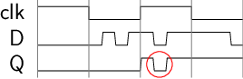 |
|---|
This is because latches are level-triggered storage elements. As long as the input changes, the latch can immediately feel it and spread the change to the output. In contrast, we need an edge-triggered storage element,which only spread the input to the output when the signal edge arrives.
D Flip-Flop
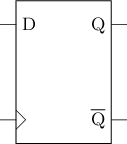
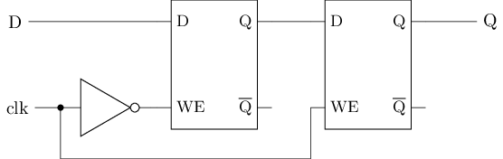
A D flip-flop is a edge-triggered storage element. It is based on latch, but can cleverly block the propagation of input signals when the clock signal is maintained at a certain level. The logic symbol of a D flip-flop is shown in the picture below, where the > symbol in the lower left corner indicates that this port needs to be connected to the clock signal. There are various implementations of the D flip-flop. Here, we first introduce the master-slave D flip-flop, whose structure is shown in the picture below.
 |  |
|---|
A master-slave D flip-flop consists of two D latches, with the left one referred to as the master latch and the right one as the slave latch. The write enable pins of the two D latches are connected to the clock signal and its inverted output, respectively. The operation of the master-slave D flip-flop is divided into the following stages:
- Data preparation stage. At this time, the clock signal
clkis at a low level, so the write enable pin of the master latch is active, and the data signalDcan enter the master latch from the outside; however, since the write enable pin of the slave latch is inactive, the data signal can't spread to the slave latch, so the output pinQof the entire D flip-flop remains unchanged. - Sampling phase. When the rising edge of the clock signal
clkarrives,the write enable pin of the master latch is inactive, so the data signalDcan't enter the master latch from the external source and any subsequent changes toDwill not affect the master latch,thereby "locking" the external dataDfrom before the rising edge of the clock signal into the master latch. At the same time, the write enable pin of the slave latch becomes active and the data "locked" in the main latch is spread to the slave latch, serving as the output of the entire D flip-flop. - Hold phase. At this time, the clock signal
clkis at a high level, so the write enable pin of the master latch is inactive and isn't affected by changes in the data signalD; although the write enable pin of the slave latch is active, since the master latch remains unchanged,the slave latch also remains unchanged, and thus the output pinQof the entire D flip-flop remains unchanged.
 |
|---|
Overall, when the rising edge of the clock arrives, data is written into the D flip-flop and the data can be read out stably in subsequent clock cycles, meeting the requirements of synchronous circuits for storage elements. Therefore, D flip-flop is basic storage elements in synchronous circuit design.
Build a D flip-flop
Try to build a D flip-flop in Logisim using gate circuits. After building it, connecting the clock port to a button. Pressing and releasing the button will generate high and low voltage levels, respectively. Therefore, clicking the button once generates a pulse, which serves as a clock signal. Try pressing down the button to observe the operation of the master-slave D flip-flop.
Build a D flip-flop with reset function
Try to add a reset input and reset function to the D flip-flop. When the reset signal is active, the value stored in the D flip-flop will become 0.
Implementing bit flip functionality using D flip-flops
Instantiate a D flip-flop with reset functionality, and invert its output before using it as input. We expect to see the output of the D flip-flop oscillate between 0 and 1. Try to compare the results with those of the D latch described above.
Build a D flip-flop triggered by a falling edge
The master-slave D flip-flop described above is triggered by a rising edge. Try to build a D flip-flop that is triggered by a falling edge. After building it, using simulation to check whether your design is correct.
Another implementation of the D flip-flop
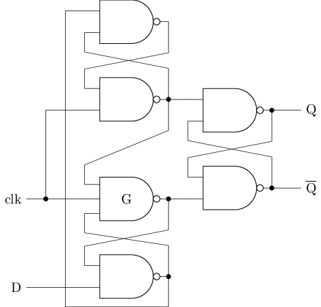
The picture below shows another implementation of a D flip-flop, known as a hold-block D flip-flop. Compared to a master-slave D flip-flop, it has more relaxed restrictions on the input. Interested students can refer to relevant materials to understand and analyze the behavior of a hold-block D flip-flop.
 |
|---|
Sometimes we don't want to unconditionally update the D flip-flop, so we need to add an enable pin to the D flip-flop to form a D flip-flop with an enable pin. Its logic symbol is shown in the picture below.
 |
|---|
Build a D flip-flop with an enabling pin
Try to build a D flip-flop with an enable pin in Logisim using D flip-flops and several circuits. After building it, checking if your solution is correct through simulation.
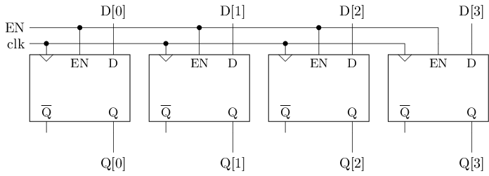
Register
The above D flip-flop can only store 1 bit of data, but sometimes it is necessary to store and process multiple bits of data as a whole. Register is a storage element composed of multiple D flip-flops, and its circuit structure is shown in the picture below. These D flip-flops share the same clock signal and enable signal, thereby achieving the effect of overall storage.
 |
|---|
Build a 4-bit register
Try to build a 4-bit register with reset function in Logisim using D flip-flops. After building it, try to write 4-bit data to the register from the DIP switch and connect the register output to a seven-segment display for display.
Build a 4-bit counter
Using the above four registers and the previously constructed adder, implement a four-bit counter. Each time a clock signal arrives, the value in the register is incremented by one. When the maximum value is reached, the counter resets to 0. In Logisim, you can instantiate a constant using the Constant component under the Wiring category in the component library. For specific usage instructions,please RTFM.
Design a circuit for summing sequences
Try to calculate the result of 1+2+...+10 using registers and adders. To accommodate the calculation results, you may consider implementing 8-bit registers and adders.
Implement an electronic clock
Using registers and seven-segment display, implementing an electronic clock with "minutes" and "seconds" functions.
Hint: The Clock component can automatically generate clock signals without the need for manual clicks like buttons. You can find it in the Wiring category of the Logisim component library. For specific usage instructions, please RTFM.