F5 Simple Processor Supporting Sequence Summation
Through ISA and state machine models, we have learned how programs are executed. In addition, we have also learned the basics of digital logic circuits. Now it's time to implement a CPU using digital circuits!
Before that, we need to clarify the details of the instruction set sISA that we need to implement. Compared with the previous subsection, some register bit widths are also specified here:
- PC bit width is 4 bits, initial value is
0 - There are 4 GPRs, each with a bit width of 8 bits
- Supports the following 3 instructions
 7  6 5  4 3   2 1   0
+----+----+-----+-----+
| 00 | rd | rs1 | rs2 | R[rd]=R[rs1]+R[rs2]      ADD instruction for register addition
+----+----+-----+-----+
| 10 | rd |    imm    | R[rd]=imm               LI instruction (Load Immediate with zero-extension)
+----+----+-----+-----+
| 11 |   addr   | rs2 | if (R[0]!=R[rs2]) PC=addr BNER0 instruction (Branch if Not Equal to Register 0)
+----+----------+-----+
We refer to this CPU, which implements the sISA instruction set using digital circuits, as sCPU. To implement sCPU, we need to implement every concept in sISA using digital circuits. For simplicity, let's start with the simplest li instruction,that is, let's first implement an sCPU that only supports the li instruction.
sCPU with only one instruction
Let's first review the specific process of executing a li instruction using the ISA state machine model.
In fact, regardless of the instruction being executed, the steps are similar.
There is a concept called the ‘instruction cycle’ that specifically describes these steps:
- Fetch: Based on the current PC, locate an instruction in memory.
- Decode: Determine the specific type of instruction and its operands
- For example, with the
liinstruction, the operand requires checking the immediate value and determining which destination register to write to
- For example, with the
- Execute: Process the operands and update the specified destination register if necessary
- Update PC: Set the PC to point to the next instruction
Therefore, our goal is to implement each of these steps using digital circuits.
Fetch
First, you need a PC register. You have already implemented registers using digital circuits, so the PC register is not difficult to implement. Then, you need to find an instruction in the memory based on the PC, so you also need to implement the memory.
Both memory and registers can store information, but memory also supports addressing. That is, the contents of memory are arranged in order; given an address, memory can read out the content corresponding to that address. We can regard memory as a matrix composed of bits, where each row of the matrix is called a memory word, the address is the row number, and the number of rows is called the memory depth. Typically, a memory word contains multiple bits of data, and its bit-width is called the memory width. Memory specifications are usually expressed as depth x width. For example, a 2x3 memory is arranged as follows, where represents the bit stored in the row and column
| Address | Memory Word |
|---|---|
| 0 | |
| 1 |
Functionally, memory can be categorized into Read-Only Memory (ROM) and Random Access Memory (RAM). The former does not support write operations, while the latter does. For sISA, since none of its three instructions access memory (only instruction fetch requires reading instructions from memory), ROM can be implemented here.
The structure of a 2x3 ROM is shown in the figure below. The decoder at the upper left is called the 'address decoder', and the wires connected to the address decoder outputs are called 'word lines'. Each word line performs an AND operation with the memory cells in the corresponding memory word, then the results of the AND gates in the same column undergo an OR operation. The wires connected to the OR gate outputs are called 'bit lines'.
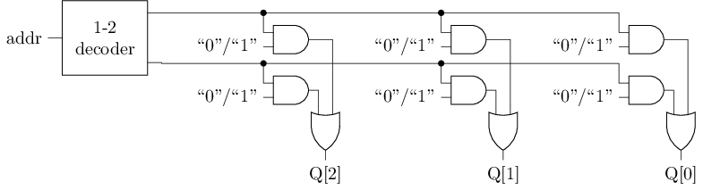 |
|---|
Given an address addr, the corresponding memory word can be read from the ROM through the following process: The address decoder converts the input address into a one-hot code. Since only one bit is active in the one-hot encoding, among all word lines, only the word line corresponding to addr becomes active. This enables the stored information in that row to pass through the AND gates. Information in other rows is filtered to 0 by the AND gates due to their inactive word lines. Each bit of the selected memory word is then transmitted through the OR gates to the bit lines, outputting the data externally from the memory.
Functionally, the address decoder, AND gates, and OR gates in the diagram collectively form a 3-bit 2-to-1 multiplexer. Consequently, reading from ROM can be viewed as selecting one memory word from multiple stored words, where the address addr acts as the multiplexer's selection input, and all memory words serve as its data inputs. Notably, information stored in ROM is directly encoded using voltage levels (high/low), making the ROM functionally equivalent to a multiplexer with constant data inputs.
Implement Instruction Fetch Function
Implement a ROM using multiplexers to store the summation sequence instructions, then retrieve instructions via the PC Register. You need to determine the ROM specifications based on your understanding.
Decode
When executing instructions on the ISA state machine, we identify functionality either directly through assembler representations (e.g., li r0, 10) or by decoding binary instruction formats (e.g., 10001010) using functional specifications - both being manual decoding approaches. Now we must implement this process in hardware circuits. Crucially, since instructions are stored in binary within circuits, we need to perform instruction decoding at the binary level.
However, since only the li instruction needs implementation currently, we can assume all fetched instructions are li with no other cases. At this stage, we simply need to extract the rd and imm fields from the li instruction. From a circuit perspective, this requires only bit-field extraction operations, which are straightforward to implement.
Execute
The li instruction loads the immediate value imm into the rd register. Consequently, we must address the implementation of the ISA's General-Purpose Registers.
Typically, a GPR set contains multiple registers, with each access targeting only specific registers. Thus, the GPR must support addressing. This reveals that the GPR circuit is fundamentally a memory device. However, since GPRs serve as destination registers for instruction writes, they require writable memory functionality—making them RAM.
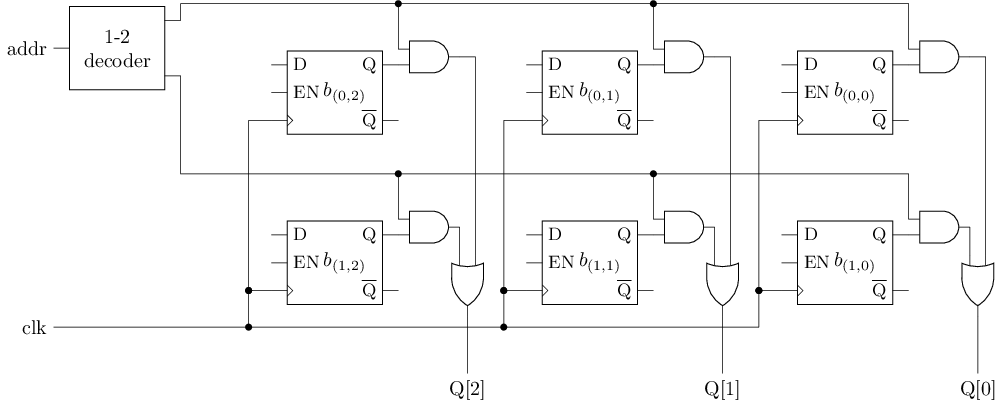
Consider a 2×3 RAM whose read operation structure is shown in the figure below. Observe that except for the storage cells being implemented with D flip-flops, the remaining structure mirrors that of a ROM. Consequently, the read operation workflow of RAM can reference the description in the aforementioned ROM section.
 |
|---|
For RAM write operations, the involved structure is shown in the figure below. Performing a write requires not only an address but also the data to be written D. Since RAM doesn't require writing at all times (e.g., during bner0instruction execution, GPR writes are unnecessary), a write enable signal EN is essential to indicate whether writing should occur.
 |
|---|
Given an address addr and write data D, when write enable EN is active, data D can be written to the corresponding memory word in RAM. The process operates as follows: Write data D connects each bit to the D-inputs of all memory cells in corresponding bit positions via bit lines. The enable signal EN filters the one-hot code output from the address decoder through an AND gate and connects to the word line. Consequently when EN is active, only the word line for addr asserts while others remain deasserted. Each row's word line connects to the enable (EN) input of its memory cells, causing the selected memory word to latch write dataD at the next clock edge, completing the write operation.
The structure of RAM shown in the following figure is obtained by combining the read and write operation structures. This type of RAM can only access one memory word via one address at any given time, thus being referred to as "single-port RAM". Correspondingly, some RAMs can access multiple memory words through multiple addresses simultaneously, which are called "multi-port RAMs". It is evident that increasing the number of "ports" in RAM requires adding extra circuit logic to enable the circuit logic of multiple ports to operate concurrently.
 |
|---|
Similar to ROM, the address decoder, the AND gates and OR gates in the read operation path in the diagram collectively form a 3-bit 2-to-1 multiplexer in terms of functionality. Therefore, the read function of RAM can also be regarded as a multiplexer with registers as its data terminals, while the write function needs to be additionally implemented on the basis of registers.
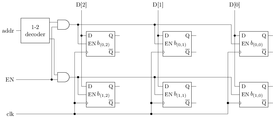
Implement GPR and its write function
Build a RAM based on registers to realize the write function of GPR. You need to determine the specifications of RAM according to your understanding.
Update PC
Updating the PC is a very simple operation, which only requires incrementing the PC register by 1. This can be achieved using a counter in digital circuits.
Implement an sCPU that only supports the li instruction
Based on the above, implement each component involved in the instruction cycle of li using digital circuits and connect them together. After implementation, try to make the sCPU execute the first few li instructions in the sequence summation program,and observe whether the state of GPR in the circuit is consistent with the state specified by the ISA.
Implementing a Complete sCPU
Next, consider how to implement the add instruction. Since for all instructions, the two steps of instruction fetch and PC update behave the same way, we can directly reuse the previously implemented instruction fetch logic.
For decoding, since the behavior of the add instruction differs from that of the li instruction, it is necessary to identify which instruction is currently fetched. To achieve this, we need to check the opcode field of the instruction: if it is 00, it is an add instruction; if it is 10, it is an li instruction. The most suitable circuit for identifying the value of an input is a decoder! Since the opcode is only 2 bits, we can use a 2-4 decoder. The one-hot code it outputs can indicate the type of the current instruction, and such a decoder is called an instruction decoder. This set of one-hot codes usually serves as control signals to control how part of the circuit works, thereby supporting the functions of different instructions.
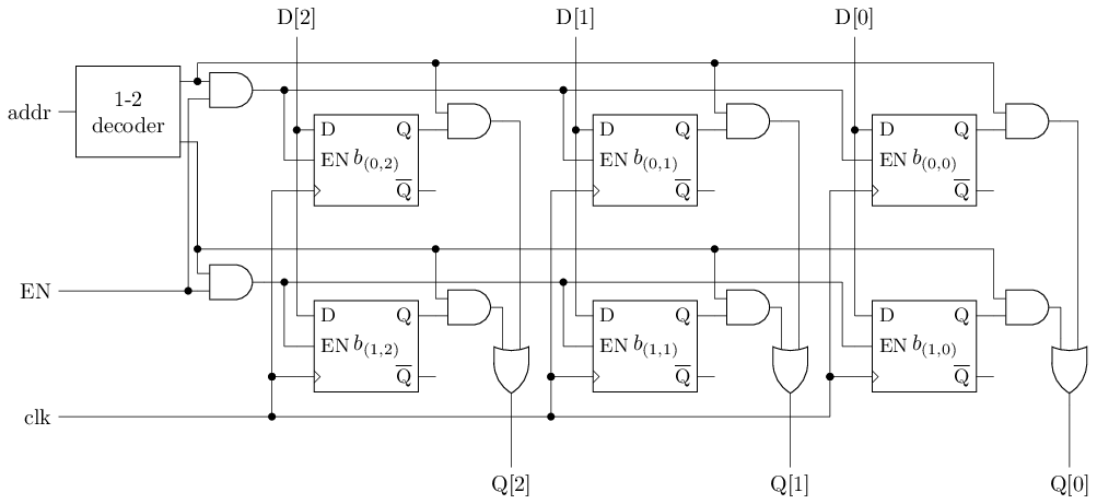
After considering the operation code, we also need to take the operands into account. Compared with the li instruction, the add instruction not only needs to write to rd, but also needs to read rs1 and rs2 as source operands, requiring simultaneous access to GPR through two read ports and one write port. Therefore, we also need to add two read ports to GPR. After adding, the GPR module should contain at least the following port signals:
- 1st read port:
raddr1(read address),rdata1(read data) - 2nd read port:
raddr2,rdata2 - Write port:
waddr(write address),wdata(write data),wen(write enable),clk(clock)
After reading out the source operands, the behavior of the add instruction is to add the two numbers and then write the addition result to the rd register. The former can be implemented via an adder, but when the latter writes to GPR, the wdata port of GPR is already occupied by the result of the li instruction. Considering the uniqueness of instruction opcode encoding, an instruction cannot be both an li instruction and an add instruction. Therefore, the data to be written to GPR can be selected based on the instruction type: if the current instruction is an add instruction, the result of the adder is selected; otherwise, the immediate value of the li instruction is selected. Such a selection function can be implemented through a multiplexer: take the two data sources to be written to GPR as the data terminals of the multiplexer, and then connect the appropriate signal from the one-hot code during decoding to the select terminal of the multiplexer. This allows the multiplexer to select the correct data according to the instruction type, thereby realizing the aforementioned function.
Add the add instruction
Based on the above, add the add instruction to the sCPU. After implementation, try to make the sCPU continue executing several add instructions in the sequence summation program, and observe whether the state of GPR in the circuit is consistent with the state specified by the ISA.
Finally, there is the bner0 instruction. To identify the bner0 instruction, we can reuse the functionality of the instruction decoder. As for operands, in addition to rs2 and addr in the instruction, there is also an implicit R[0]. Since the position of the rs2 field in the bner0 instruction is the same as that in the add instruction, we can reuse the logic for reading the rs2 register from the add instruction. However, bner0 also needs to read out R[0], so 0 can be used as the input to the raddr1 port of GPR. This port is already occupied by rs1 of the add instruction, but this issue can similarly be resolved using a multiplexer.
After reading out the source operands, the bner0 instruction needs to compare whether the two numbers are equal, which can be implemented by a comparator. If the comparison result is not equal, the PC needs to be updated to the addr field. In other words, only when the current instruction is a bner0 instruction and the comparison result is not equal, the PC is updated to the addr field; in all other cases, the PC should be updated to PC plus 1. Similarly, we can use a multiplexer to select the input of the PC register. Finally, the bner0 instruction does not write to GPR, so the wen of GPR needs to be set to invalid.
Add the bner0 instruction
Based on the above, add the bner0 instruction to the sCPU. After implementation, try to make the sCPU execute the complete sequence summation program. If your implementation is correct, you should see that the PC is finally 7 and the summation result 55 is stored in a certain GPR
Compare with the sequence summation circuit
When studying digital circuits, there is a mandatory problem that requires you to calculate the result of 1+2+...+10 using registers and adders. Now that you have completed the same calculation with the sCPU, try to compare the advantages and disadvantages of the two schemes.
Re-examining the CPU
Congratulations! This is probably the first CPU you've implemented! Although this sCPU is very simple, it allows us to glimpse some properties that help us understand CPUs. When discussing how to add instructions earlier, we first analyzed the intended behavior of each instruction, then sequentially added the required components along the direction of data flow based on the instruction's behavior. The paths through which data flows in the CPU, along with the related components on these paths, are called the CPU's data path. In the previous discussion, components belonging to the data path include GPRs, adders, memory, comparators, etc. When data path conflicts occur among multiple instructions, it is usually necessary to introduce additional circuits to control the flow of data, ensuring that each instruction can perform operations compliant with the ISA specifications. These additional circuits belong to the control logic within the CPU, and the signals that determine the behavior of the control logic are called control signals. In fact, designing the data path and control signals are precisely the two most critical steps in CPU design. We have summarized the control logic involved earlier and their intended behaviors when executing different instructions as follows:
| Instruction | wdata Selection | wen | raddr2 Selection | PC Update Selection |
|---|---|---|---|---|
add | Adder output | 1 | Instruction's rs2 | PC + 1 |
li | Immediate value | 1 | X | PC + 1 |
bner0 | X | 0 | 0 | 指令的addr |
Among them, X denotes a don't care, meaning any selection is acceptable. For example, the bner0 instruction does not write to GPR, so regardless of what is selected for wdata, it does not affect the correctness of the sCPU. It should be noted that these selections are related to the type of instruction; that is, the type of instruction determines the behavior of the control logic, which in turn determines the direction of data flow in the data path, and ultimately accomplishes the function specified by the instruction. Looking at the sCPU you designed in Logisim, if you take the fetched instruction as a boundary and divide the sCPU into left and right sides, you should find that the only information transmitted from the left side to the right side is the instruction. At the same time, the control logic of the right-side circuit is ultimately controlled by the one-hot code output by the instruction decoder, and the input terminal of the instruction decoder is the opcode of the instruction. Therefore, it can be said that the right-side circuit is completely controlled by the instruction. This exactly confirms what was stated in the previous section: "Executing a program on the CPU = using the instruction sequence compiled from the program to control the CPU circuit to perform state transitions." Finally, we will deepen our understanding of instructions through some mandatory exercises.
Calculate the sum of odd numbers within 10
Write a sequence of instructions to calculate the sum of odd numbers within 10, i.e.,1+3+5+7+9. Then try to execute this instruction sequence with the sCPU you designed and check if the running result meets the expectations. After completion, what understanding do you have of the computer's "stored program" idea?
Add a new instruction
Try to add a new instruction out rs to sISA. When this instruction is executed, it will output R[rs] in hexadecimal form to the seven-segment display. You can determine the encoding of this instruction by yourself. Then, implement theoutinstruction in the sCPU and modify the sequence summation program so that the calculation result can be displayed on the seven-segment display after it is calculated.
Is it possible to design an instruction that adds 10 numbers?
The sequence summation program mentioned above requires dozens of instructions to compute the result. A classmate suggested that, in order to improve the computing efficiency of the sCPU, an instruction that adds 10 numbers should be designed, so that 1+2+...+10 can be directly computed with a single instruction. Is this suggestion reasonable? Try to provide your reasons from the perspectives of programs, ISA, and CPU circuit design.