
F6 Простой ввод/вывод
Вы уже спроектировали sCPU в Logisim и выполнили программу суммирования последовательности. Чтобы проверить результаты выполнения, вы напрямую наблюдали значения регистра PC и GPR. Однако в реальном процессорном чипе напрямую наблюдать внутреннее состояние крайне сложно. На практике пользователи обычно взаимодействуют с процессорными чипами через ввод/вывод (input/output, I/O).
Расширение набора инструкций sISA
У кода операции sISA всё ещё остаётся один свободный слот. Мы можем расширить sISA, добавив новую инструкцию io, что позволит sCPU поддерживать функциональность ввода/вывода. Одновременно, чтобы sISA могла беспрепятственно поддерживать более сложные программы, нам нужно усилить функциональность инструкций li и bner0. Итоговая sISA включает следующие четыре инструкции:
 7  6  5  4  3   2  1   0
+--+--+--+--+---+--+--+--+
| 00 | rd | rs1 | rs2 | R[rd]=R[rs1]+R[rs2]
+--+--+--+--+---+--+--+--+
| 01 | rd |i/o|  idx  | R[rd]<=>dev[idx]
+--+--+--+--+---+--+--+--+
| 10 | rd | s |  imm  | R[rd]=imm << (s << 1)
+--+--+--+--+---+--+--+--+
| 11 |  offset  | rs2 | if (R[0]!=R[rs2]) PC=PC+sign_ext(offset)
+--+--+--+--+---+--+--+--+
Здесь:
- Поведение инструкции
addостаётся таким же, как и раньше. - Инструкция
ioвыполняет ввод или вывод в зависимости от бита направленияi/o:- Когда
i/o=0, это означает операцию ввода: из устройства с номеромidxсчитываются 8-битные данные и записываются вR[rd]. - Когда
i/o=1, это означает операцию вывода: 8-битные данные изR[rd]отправляются в устройство с номеромidx.
- Когда
- Инструкция
liотличается от прежней версии: она использует комбинациюsиimm, чтобы представить более широкое непосредственное значение. Упомянутый выше символ<<обозначает оператор сдвига влево. Если вы не вполне знакомы с этим оператором, поведение инструкцииliможно понять и иначе:sуказывает, в какой сегмент 8-битных данных помещается 2-битное значениеimm, как подробно показано в следующей таблице:
 7   6 5   4 3   2 1   0
+-----+-----+-----+-----+
| 00  | 00  | 00  | imm | s=00
+-----+-----+-----+-----+
| 00  | 00  | imm | 00  | s=01
+-----+-----+-----+-----+
| 00  | imm | 00  | 00  | s=10
+-----+-----+-----+-----+
| imm | 00  | 00  | 00  | s=11
+-----+-----+-----+-----+
- Инструкция
bner0отличается от прежней версии: она использует полеoffset, чтобы представить смещение цели перехода относительно PC, тем самым поддерживая переходы к местам вблизи текущего значения PC. При этом полеoffsetможет представлять отрицательные числа, позволяя переходить к местам в диапазоне от-8до+7относительно текущего значения PC.
Прежде чем добавлять инструкцию io, сначала усилим функциональность инструкций li и bner0. Для инструкции li нужно рассмотреть, как реализовать функциональность поля s. На самом деле, поле s можно рассматривать как сигнал выбора, чтобы выбрать одно из четырёх непосредственных значений, где каждое непосредственное значение соответствует сценарию размещения imm в определённом сегменте. С этой точки зрения функциональность инструкции li можно реализовать с помощью мультиплексора.
Для инструкции bner0, поскольку поле offset представляет лишь смещение цели перехода относительно PC, чтобы получить фактическую цель перехода, значение PC нужно сложить с полем offset. Операцию сложения можно реализовать с помощью сумматора. Ранее сумматор уже использовался для вычисления PC+1; учитывая, что при выполнении перехода инструкцией bner0 вычислять PC+1 не нужно, можно рассмотреть возможность повторного использования этого сумматора для вычисления цели перехода. Однако для повторного использования нужно продумать, как добавить дополнительные управляющие сигналы.
Тем не менее, поскольку регистр PC имеет 8 бит, а поле offset инструкции bner0 — только 4 бита, прежде чем выполнять сложение, offset сначала нужно расширить до данных, соответствующих разрядности PC. Обычно применяются два способа расширения. Один — расширение нулями, при котором в старшие разряды всегда добавляется 0; именно расширение нулями требуется для непосредственного значения инструкции li. Другой — расширение знака, при котором в старшие разряды добавляется знаковый разряд числа в дополнительном коде.
В частности, можно также доказать, что до и после расширения знака истинное значение числа в дополнительном коде остаётся неизменным. Пусть есть -битное двоичное число . Расширив его знаком до бит, получаем . Если , истинные значения до и после расширения, очевидно, совпадают. Если , разложив по весам разрядов дополнительного кода, получаем:
Легко видеть, что приведённый выше вывод выполняется при . По принципу математической индукции утверждение доказано.
F: Реализуйте усиленные версии инструкций
Измените реализацию sCPU, чтобы она поддерживала усиленные версии инструкций li и bner0.
Затем измените последовательность инструкций программы суммирования последовательности так, чтобы программа использовала усиленные инструкции для вычисления 1+2+...+10. Заставьте sCPU выполнить изменённую программу суммирования последовательности и проверьте, верен ли результат суммирования.
Добавление в sCPU поддержки ввода/вывода
Теперь мы можем добавить в sCPU несколько простых устройств, затем реализовать инструкцию io и, наконец, позволить программе с помощью инструкции io обращаться к этим устройствам.
LED
Создайте экземпляр компонента LED Bar в Logisim; его можно найти в категории Input/Output библиотеки компонентов. После создания настройте его свойства: установите свойство Input Format в One Wire, а свойство Segments — в 8. Таким образом мы получаем 8 LED, управляемых 8-битным сигналом, где каждый бит сигнала может управлять состоянием включения/выключения соответствующего LED.
Мы хотим, чтобы программа могла управлять LED с помощью 8-битных данных. Например, использование результата вычисления 1+2+...+10 для управления LED позволяет добиться эффекта «вывода результата вычисления на LED». Для этого нам нужно добавить инструкцию io; когда программа выполняет инструкцию io, sCPU может использовать указанные данные для управления LED.
Обычно устройств больше одного, и для их различения обычно используются разные номера. Программа может указывать, к какому устройству обращаться, через поле idx инструкции io. Мы условимся, что при использовании инструкции io для вывода номер 000 обозначает LED.
Кроме того, при использовании инструкции io для вывода поле rd инструкции нужно считать как номер регистра-источника. Однако добавлять к GPR отдельный порт чтения специально для этого случая (например, добавляя raddr3 и rdata3) невыгодно. На самом деле инструкция io не использует поля rs1 и rs2 для обращения к GPR. Поэтому мы можем повторно использовать существующие порты чтения GPR, добавив правильные управляющие сигналы, чтобы выбрать поле rd инструкции в качестве адреса для одного из портов чтения GPR.
Наконец, мы ожидаем, что состояние включения/выключения LED останется неизменным после выполнения инструкции io. Если GPR, указанный в инструкции io, подключить к LED напрямую, состояние включения/выключения LED будет меняться при следующем изменении значения, хранимого в этом GPR, даже если инструкция io не выполняется. Это не соответствует нашим ожиданиям. Чтобы решить эту проблему, нам нужно добавить для LED дополнительный выходной регистр данных. С одной стороны, подключите выход этого выходного регистра данных к LED; с другой стороны, пусть инструкция io записывает данные, используемые для управления LED, в этот выходной регистр данных. Таким образом значение выходного регистра данных может оставаться неизменным, тем самым сохраняя состояние включения/выключения LED.
Выведите результат вычисления на LED
Добавьте инструкцию io в sCPU, чтобы инструкция io могла управлять LED.
Затем измените последовательность инструкций программы суммирования последовательности, чтобы программа выводила результат вычисления на LED с помощью инструкции io, и проверьте, соответствует ли состояние включения/выключения LED ожиданиям.
Семисегментный индикатор
Семисегментный индикатор, который мы использовали ранее, принимает 7-битный входной сигнал, где каждый бит по отдельности управляет состоянием включения/выключения соответствующего сегмента. Есть и другой тип семисегментного индикатора, который принимает 4-битный входной сигнал и напрямую отображает шестнадцатеричную цифру, соответствующую 4-битному двоичному числу; его использование позволяет сэкономить на процессе декодирования.
Создайте экземпляры двух компонентов Hex Digit Display в Logisim; их можно найти в категории Input/Output библиотеки компонентов. После создания настройте их свойства: установите свойство Has Decimal point: в No. Мы можем разбить 8-битный сигнал на два 4-битных сигнала, чтобы по отдельности управлять двумя семисегментными индикаторами, что эквивалентно преобразованию 8-битного двоичного числа в 2-разрядное шестнадцатеричное число для отображения. Мы условимся, что при использовании инструкции io для вывода номер 001 обозначает эту группу семисегментных индикаторов.
Выведите результат вычисления на семисегментные индикаторы
Завершите реализацию инструкции io, чтобы инструкция io могла управлять семисегментными индикаторами. Как и для LED, вам также нужно добавить выходной регистр данных для семисегментных индикаторов.
Затем измените последовательность инструкций программы суммирования последовательности так, чтобы программа выводила результат вычисления на семисегментные индикаторы с помощью инструкции io, и проверьте, соответствует ли состояние отображения семисегментных индикаторов ожиданиям. Учтите, что компонент Hex Digit Display отображает значения в шестнадцатеричном виде.
DIP switch
Создайте экземпляр компонента Dip switch в Logisim; его можно найти в категории Input/Output библиотеки компонентов. После создания настройте его свойства: установите свойство Number of Switch в 8. Эти 8 DIP switch можно объединить в 8-битный входной сигнал. Мы условимся, что при использовании инструкции io для ввода номер 000 обозначает эту группу DIP switch.
На первый взгляд номер устройства для DIP switch совпадает с номером LED, но, поскольку DIP switch — это устройство ввода, а LED — устройство вывода, их можно дополнительно различить через бит направления i/o в инструкции io.
Кроме того, при использовании инструкции io для ввода значение соответствующего устройства нужно записать в регистр rd. Вам нужно изменить тракт данных и добавить соответствующие управляющие сигналы, чтобы реализовать функциональность ввода.
Ранее программа суммирования последовательности всегда вычисляла 1+2+...+10. Если нужно было изменить последний член последовательности, новый последний член приходилось вручную загружать в r0. На самом деле мы можем заранее установить последний член на DIP switch, а затем заставить программу в начале выполнения считать последний член с DIP switch с помощью инструкции io, прежде чем переходить к вычислению.
В отличие от устройств вывода, таких как LED, состояние устройства ввода задаётся пользователем и не подвержено влиянию внутреннего состояния процессора. Поэтому для устройств ввода не нужно добавлять регистры для временного хранения их состояния.
Считайте последний член последовательности с DIP switch
Завершите реализацию инструкции io, чтобы инструкция io могла считывать данные с DIP switch в GPR.
Затем измените последовательность инструкций программы суммирования последовательности так, чтобы программа считывала последний член с DIP switch с помощью инструкции io, и проверьте, соответствует ли результат вычисления ожиданиям, с помощью LED или семисегментных индикаторов.
Ситуация, когда последний член равен 0
Когда введённый последний член равен 0, каким будет результат выполнения программы? Почему так происходит?
Однако мы не требуем от вас исправлять эту проблему.
Кнопка
Создайте экземпляры 8 компонентов Button в Logisim; их можно найти в категории Input/Output библиотеки компонентов. Эти 8 кнопок можно объединить в 8-битный входной сигнал, где нажатая кнопка означает, что соответствующий бит равен 1, а отпущенная — что соответствующий бит равен 0. Мы условимся, что при использовании инструкции io для ввода номер 001 обозначает эту группу кнопок.
Управляйте отображением результатов с помощью кнопок
Завершите реализацию инструкции io, чтобы инструкция io могла считывать данные с кнопок в GPR.
Затем измените последовательность инструкций программы суммирования последовательности так, чтобы во время цикла текущий член выводился на LED. После завершения вычисления программа должна непрерывно опрашивать состояние кнопок, пока не будет нажата кнопка, и только после этого семисегментные индикаторы должны показать результат вычисления. Проверьте, соответствует ли поведение кнопки ожиданиям.
Реализуйте пошаговое суммирование
Измените последовательность инструкций программы суммирования последовательности, чтобы одновременно добиться следующих эффектов:
- На каждой итерации цикла выводить текущий член на LED, а текущий результат суммирования — на семисегментные индикаторы.
- Использовать кнопку для управления ходом цикла; программа переходит к следующей итерации цикла только при каждом нажатии кнопки, представляющей младший бит.
То есть при запуске программы LED и семисегментные индикаторы сначала показывают 1 и 1; после того как пользователь нажмёт кнопку, представляющую младший бит, LED и семисегментные индикаторы показывают 2 и 3; после того как пользователь снова нажмёт кнопку, представляющую младший бит, LED и семисегментные индикаторы показывают 3 и 6...
Поскольку GPR всего 4, а диапазон смещения, который может вместить инструкция bner0, — только от -8 до 7, вам может понадобиться тщательно продумать распределение GPR, чтобы максимально уменьшить число инструкций в цикле и гарантировать, что смещение цели перехода bner0 не выходит за пределы диапазона, представимого инструкцией.
Подсказка: есть решение, требующее всего 12 инструкций.
Реализуйте пошаговое суммирование (2)
Вы можете заметить, что если пользователь непрерывно удерживает кнопку нажатой, не отпуская её, ход цикла будет продолжать продвигаться вперёд. Если вы хотите, чтобы программа переходила к следующей итерации цикла только тогда, когда пользователь один раз нажмёт и отпустит кнопку, сможете ли вы написать программу, удовлетворяющую этому требованию? Почему?
На пути к современному проектированию процессоров
Поздравляем, вы успешно спроектировали в Logisim процессор с некоторыми демонстрационными возможностями. Но в то же время вы, вероятно, уже почувствовали, что у проектирования процессора в Logisim есть немало недостатков:
Громоздкое проектирование. Хотя перетаскивание компонентов и их соединение проводами действительно даёт ощущение проектирования схемы, эти операции становятся громоздкими по мере роста масштаба проекта. У спроектированного вами сейчас процессора sCPU всего 4 инструкции, но у процессора с относительно полной функциональностью обычно десятки инструкций; чтобы реализовать процессор, способный загрузить современную операционную систему, нужно реализовать сотни инструкций. Если же рассмотреть зрелые коммерческие процессоры вроде современных Intel и ARM, им нужно поддерживать тысячи инструкций, одно только руководство по ISA насчитывает тысячи страниц, а число транзисторов на чипе достигает масштаба десятков миллиардов.
Низкая скорость моделирования. С одной стороны, эффективность моделирования самого Logisim невысока, и по мере усложнения масштаба проекта скорость моделирования будет становиться всё медленнее из-за роста числа компонентов. С другой стороны, при одинаковой функциональности программы, когда ISA предоставляет меньше типов инструкций, для её реализации программе обычно требуется больше инструкций, что снижает эффективность выполнения в несколько раз, а то и в десятки раз.
Сложная отладка. Стоит всего одному проводу оказаться случайно неправильно подключённым в процессе проектирования, и результат выполнения программы на процессоре может не соответствовать ожиданиям. Если масштаб программы невелик, мы всё ещё можем проверять состояние выполнения процессора инструкция за инструкцией, сверяя его с состоянием ISA; но когда программе нужно выполнить тысячи или десятки тысяч инструкций, найти, при выполнении какой инструкции результат не совпал с ожиданиями, чрезвычайно сложно. Если бы вы запустили настоящее приложение вроде игры, число выполненных инструкций было бы астрономическим! Найти ошибку среди такого количества инструкций попросту сложнее, чем найти иголку в стоге сена!
Все эти проблемы говорят о том, что проектирование процессора с помощью Logisim — не слишком масштабируемое решение. На самом деле, в современных потоках проектирования процессоров в основном применяется подход разработки через код: используется язык описания аппаратуры (Hardware Description Language, HDL) для описания того, как соединены аппаратные компоненты, тем самым задавая логическую структуру процессора без необходимости вручную выполнять соединения проводами. После завершения разработки кода нужны инструменты моделирования, чтобы проверить, соответствует ли логическая структура, заданная кодом, ожиданиям. Кроме того, нужны EDA-инструменты, чтобы преобразовать код в топологию, подобно тому, как компилятор преобразует код на C в последовательность инструкций.
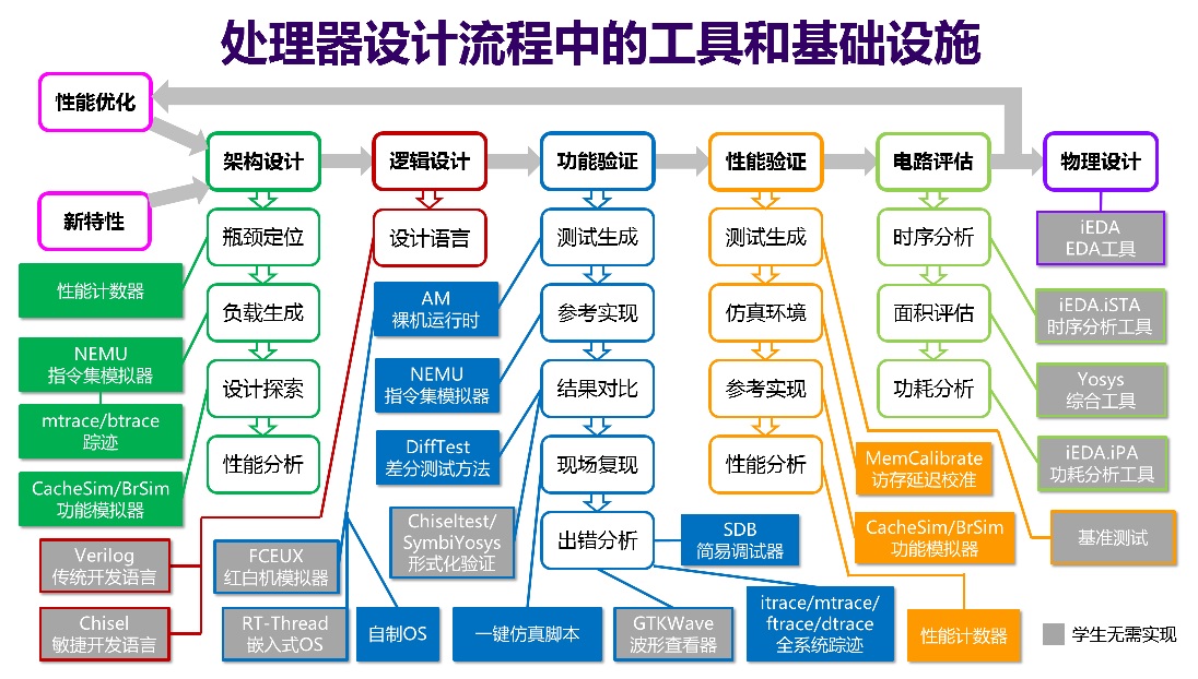
Помимо описанных выше шагов, современные потоки проектирования процессоров охватывают и другие этапы, как показано на рисунке ниже. Перечислим часть проблем, которые нужно решить в современном потоке проектирования процессоров:
- Архитектурное проектирование: имея новую функцию (это может быть функциональность из спецификации ISA, например добавление новых инструкций, или схема функциональной оптимизации на уровне процессора), как предложить проектное решение и разбить его на подходящие аппаратные модули для реализации?
- Логическое проектирование: имея проектное решение, как реализовать аппаратные модули этого решения на уровне схемы с помощью HDL?
- Функциональная верификация: как проверить, что схема, описанная на HDL, удовлетворяет ожидаемой функциональности новой функции?
- Верификация производительности: как убедиться, что производительность процессора соответствует ожиданиям?
- Оценка схемы: как оценить и оптимизировать такие показатели процессора, как частота, площадь и энергопотребление?
- Физическое проектирование: как преобразовать код на HDL в топологию, готовую к передаче в производство (tape-out)?
- Оптимизация производительности: как обнаружить и локализовать узкие места производительности в процессоре и спроектировать соответствующие схемы оптимизации?
При этом вы должны также осознавать, что даже в описанном выше процессе проектирования в Logisim остаётся ещё немало шагов, которые вы, возможно, пока не понимаете, например:
- Как эффективно получить последовательность инструкций программы?
- Как разрабатывать больше программ для запуска на процессоре?
Проектирование процессора != программирование на HDL
Многие студенты, обучающиеся по электронным специальностям, могут просто считать проектирование процессора работой по написанию кода на HDL. Этот взгляд однобок: судя по рисунку выше, программирование на HDL — это лишь работа на этапе логического проектирования, тогда как весь поток состоит из множества этапов. На самом деле многие этапы процесса проектирования процессора связаны с программным обеспечением, потому что:
Процессор не может работать без программного обеспечения. Вы уже знаете, что принцип работы процессора — это непрерывное выполнение инструкций, а эти инструкции и есть программное обеспечение. Оценить процессор — значит увидеть, правильно и хорошо ли на нём выполняется программное обеспечение.
В потоке, показанном на рисунке выше, для выполнения этих шагов требуется поддержка различных инструментов и инфраструктуры. По своей сути эти инструменты и инфраструктура тоже являются программным обеспечением, особенно те инструменты, что тесно связаны с функциональностью процессора (такие как симулятор системы команд, функциональный симулятор и методы дифференциального тестирования на рисунке); они играют важную роль в выполнении соответствующих шагов.
Хотя код на HDL описывает аппаратуру, сам по себе, будучи кодом, он тоже является разновидностью программного обеспечения. Раз это код, для управления им, его поддержки, тестирования, оценки и оптимизации нужно использовать соответствующие программные технологии. Особенно по мере роста масштаба кода эти вопросы будут становиться всё важнее. К счастью, область программной инженерии изучает эти вопросы уже десятилетиями; при необходимости мы можем опираться на опыт области программной инженерии, чтобы решать связанные с этим проблемы.
Короче говоря, чтобы спроектировать хороший процессор, нужно ценить роль, которую в нём играет программное обеспечение.
Сейчас вы, возможно, не до конца понимаете значимость упомянутых выше проблем, и мы не намерены подробно останавливаться на них здесь. В дальнейшем мы откажемся от подхода к проектированию в Logisim и будем постепенно направлять всех к построению упомянутого выше современного потока проектирования процессоров, и в этом процессе ваше понимание этих проблем тоже будет становиться всё яснее.
Вы вот-вот шагнёте в мир кода. Вы готовы?
zxz