
C5 Компьютерная система SoC
Обновление методических материалов по шине
29 ноября 2023 года мы добавили в раздел о шине упражнения по UART и CLINT. Выполнение этих упражнений будет полезно для последующей интеграции SoC.
После реализации шины мы можем подключить NPC к среде SoC проекта OSOC, готовясь к tape-out! SoC означает System On Chip («система на кристалле»), то есть SoC содержит не только процессор, но и множество периферийных устройств, а также шину, соединяющую процессор с этой периферией. Здесь мы в широком смысле рассматриваем память как разновидность устройства, поскольку для SoC память и прочие устройства в узком смысле неразличимы — все они являются адресуемыми диапазонами адресного пространства.
ysyxSoC
Мы предоставляем среду SoC, которая может работать на Verilator, под названием ysyxSoC. Мы разрешаем вам интегрироваться с ysyxSoC на раннем этапе по двум причинам: с одной стороны, чтобы помочь всем изучить её детали, а с другой — чтобы как можно раньше протестировать ваш NPC в среде SoC, тем самым сократив время между завершением оценки для tape-out и отправкой вашего кода. Разумеется, после интеграции с ysyxSoC вам всё же придётся выполнить некоторую работу по оптимизации, чтобы удовлетворить требованиям tape-out этапа B.
Введение в ysyxSoC
Сначала представим периферийные устройства, входящие в состав ysyxSoC, и соответствующие им адресные пространства.
| Устройство | Адресное пространство |
|---|---|
| CLINT | 0x0200_0000~0x0200_ffff |
| SRAM | 0x0f00_0000~0x0fff_ffff |
| UART16550 | 0x1000_0000~0x1000_0fff |
| SPI master | 0x1000_1000~0x1000_1fff |
| GPIO | 0x1000_2000~0x1000_200f |
| PS2 | 0x1001_1000~0x1001_1007 |
| MROM | 0x2000_0000~0x2000_0fff |
| VGA | 0x2100_0000~0x211f_ffff |
| Flash | 0x3000_0000~0x3fff_ffff |
| ChipLink MMIO | 0x4000_0000~0x7fff_ffff |
| PSRAM | 0x8000_0000~0x9fff_ffff |
| SDRAM | 0xa000_0000~0xbfff_ffff |
| ChipLink MEM | 0xc000_0000~0xffff_ffff |
| Зарезервировано | Остальное |
Помимо AXI, на рисунке также фигурируют такие шины, как APB, wishbone и SPI. Однако эти шины проще, чем AXI, даже проще, чем AXI4-Lite. Поскольку вы уже знаете AXI4-Lite, изучение этих шинных протоколов не составит труда, и при необходимости вы всегда можете обратиться к соответствующим руководствам.
Некоторые устройства и адресные пространства могут измениться в будущем
Чтобы добиться лучшего эффекта отображения, команда проекта OSOC занимается переработкой SoC. Некоторые устройства и адресные пространства могут измениться в будущем, а окончательное распределение адресных пространств устройств определяется версией для tape-out. Однако это не влияет на ваше текущее обучение, и вы можете спокойно игнорировать эту особенность.
Получите исходный код ysyxSoC
Вам нужно клонировать проект ysyxSoC:
cd ysyx-workbench
git clone git@github.com:OSCPU/ysyxSoC.git
Далее вы будете использовать устройства, предоставляемые ysyxSoC, для моделирования, чтобы убедиться, что NPC может корректно обращаться к устройствам в SoC. Ниже мы расскажем, как выполнить эту интеграцию.
Следует отметить, что между ysyxSoC и SoC, используемым в финальном tape-out, всё ещё есть некоторые различия. Поэтому прохождение тестов ysyxSoC не означает, что в конечном итоге будут пройдены и тесты среды моделирования SoC для tape-out. Тем не менее, проект ysyxSoC всё же может помочь заранее выявить некоторые проблемы. Если при последующей интеграции с SoC для tape-out проблемы всё же возникнут, вы можете сосредоточиться на влиянии, вызванном различиями между ними.
Для всех есть две части проекта ysyxSoC, заслуживающие внимания. Первая часть — это шина ysyxSoC, которую мы в основном реализуем с использованием фреймворка diplomacy проекта rocket-chip из open source (свободный код) сообщества, соответствующий код расположен в директории ysyxSoC/src/. С помощью diplomacy мы можем легко подключить устройство с шинным интерфейсом к ysyxSoC. Например, нам достаточно изменить всего две строки кода на Chisel, чтобы создать экземпляр устройства MROM с интерфейсом AXI, задать его адресное пространство как 0x2000_0000~0x2000_0fff и подключить его к нижестоящей части AXI Xbar. Если бы мы использовали традиционный подход на Verilog, одно только объявление портов добавило бы почти 100 строк кода, не говоря уже об изменениях в AXI Xbar.
diff --git a/src/SoC.scala b/src/SoC.scala
index dd84776c..758fb8d1 100644
--- a/src/SoC.scala
+++ b/src/SoC.scala
@@ -39,9 +39,10 @@ class ysyxSoCASIC(implicit p: Parameters) extends LazyModule {
     AddressSet.misaligned(0x10001000, 0x1000) ++    // SPI controller
     AddressSet.misaligned(0x30000000, 0x10000000)   // XIP flash
   ))
+  val lmrom = LazyModule(new AXI4MROM(AddressSet.misaligned(0x20000000, 0x1000)))

   List(lspi.node, luart.node).map(_ := apbxbar)
-  List(chiplinkNode, apbxbar := AXI4ToAPB()).map(_ := xbar)
+  List(chiplinkNode, apbxbar := AXI4ToAPB(), lmrom.node).map(_ := xbar)
   xbar := cpu.masterNode

   override lazy val module = new Impl
Вторая часть — это устройства ysyxSoC. Мы собрали ряд open source проектов контроллеров устройств, соответствующий код расположен в директории ysyxSoC/perip/. Некоторые устройства реализованы путём непосредственного создания экземпляров IP из проекта rocket-chip; такие устройства не находятся в директории ysyxSoC/perip/, и подробности можно найти в соответствующем коде в ysyxSoC/src/.
Интеграция в ysyxSoC
Поскольку SoC содержит множество устройств, свойства этих устройств могут отличаться друг от друга, что порождает некоторые новые проблемы. Например, в ysyxSoC/perip/uart16550/rtl/uart_defines.v содержится следующий код:
// Register addresses
`define UART_REG_RB `UART_ADDR_WIDTH'd0  // receiver buffer
`define UART_REG_IE `UART_ADDR_WIDTH'd1  // Interrupt enable
`define UART_REG_II `UART_ADDR_WIDTH'd2  // Interrupt identification
`define UART_REG_LC `UART_ADDR_WIDTH'd3  // Line Control
Приведённый выше код определяет адреса некоторых регистров устройства в UART. Поскольку UART расположен по адресу 0x1000_0000, адреса четырёх указанных выше регистров — это 0x1000_0000, 0x1000_0001, 0x1000_0002 и 0x1000_0003. Предположим, что UART подключён к Xbar через шину AXI4-Lite, и рассмотрим чтение содержимого приёмного буфера (receiver buffer) через AXI4-Lite. Очевидно, что сигнал araddr должен быть равен 0x1000_0000, но если вы хотите прочитать 4 байта, будут ли одновременно считаны и содержимое трёх регистров устройства, расположенных следом?
Ранее мы не рассматривали вопрос «сколько байт читать», потому что чтение памяти не изменяет состояние хранящихся в ней данных. Поэтому, сколько бы байт ни ожидал прочитать CPU, шина может за раз считать 4 или 8 байт и позволить CPU самому выбрать из них целевые данные. Это даже помогает некоторым CPU с кэшами повысить производительность: однократное чтение данных из памяти обычно занимает много времени, поэтому если полностью использовать пропускную способность шины для считывания большего объёма данных за раз, число будущих реальных обращений к памяти может сократиться.
Однако для обращений к устройствам вышеописанная предпосылка уже не выполняется: обращение к регистру устройства может изменить состояние устройства! Это означает, что для устройства чтение 1 байта и чтение 4 байт в конечном счёте могут приводить к разному поведению. Если мы не будем обращаться к регистрам устройства согласно установленным для них соглашениям, устройство может перейти в непредсказуемое состояние. Поэтому при обращении к устройствам через шину нам нужно тщательно учитывать эту особенность.
Однако шина AXI4-Lite не может решить описанную выше проблему: в её канале AR недостаточно сигналов, чтобы закодировать информацию о длине чтения, поэтому устройству остаётся только предполагать, что фактическая разрядность данных совпадает с разрядностью данных шины AXI4-Lite. Поэтому, если один запрос на чтение по шине AXI4-Lite охватывает несколько регистров устройства, это может привести к ошибкам в состоянии устройства. Именно по этой причине не все устройства подходят для подключения через шину AXI4-Lite.
Например, упомянутый выше UART нельзя подключить через шину AXI4-Lite с разрядностью данных 32 бита, потому что интервал между регистрами устройства в этом UART составляет всего 1 байт, а значит, чтение одного регистра устройства через AXI4-Lite также повлияет на состояние соседних регистров устройства, чего мы не ожидаем. А другой UART, у которого адресное пространство регистров устройства выглядит следующим образом, можно подключить через шину AXI4-Lite с разрядностью данных 32 бита, потому что интервал между этими регистрами составляет 4 байта, что как раз позволяет прочитать один из регистров, не затрагивая состояния соседних регистров.
// Register addresses
`define UART_REG_RB `UART_ADDR_WIDTH'd0  // receiver buffer
`define UART_REG_IE `UART_ADDR_WIDTH'd4  // Interrupt enable
`define UART_REG_II `UART_ADDR_WIDTH'd8  // Interrupt identification
`define UART_REG_LC `UART_ADDR_WIDTH'd12 // Line Control
Чтобы решить описанные выше проблемы AXI4-Lite, полный протокол шины AXI использует сигналы arsize/awsize для указания фактической разрядности данных и вводит понятие «узкой передачи» (narrow transfer) для описания ситуации, когда «фактическая разрядность данных меньше разрядности данных шины». Эти два понятия «разрядности данных» не полностью совпадают. А именно, разрядность данных шины статически определяется на этапе проектирования аппаратного обеспечения; она представляет собой максимальную разрядность данных одной шинной передачи и также используется для расчёта теоретической пропускной способности шины. Фактическая разрядность данных (то есть значение сигналов arsize/awsize) динамически определяется информацией о разрядности в инструкциях доступа к памяти программного обеспечения и представляет собой фактическую разрядность данных одной шинной передачи. Например, инструкция lb обращается только к 1 байту, а инструкция lw — к 4 байтам.
Благодаря сигналам arsize/awsize устройство может узнать фактическую разрядность данных, к которым нужно обратиться программному обеспечению, так что даже когда адреса нескольких регистров устройства расположены плотно, оно может обращаться только к одному из них, избегая непреднамеренного изменения состояния устройства.
Сгенерируйте Verilog-код для ysyxSoC
Сначала вам нужно выполнить некоторую настройку и инициализацию:
- Установите mill согласно документации mill
- Проверить установку можно командой
mill --version. Кроме того, проектуrocket-chipтребуетсяmillверсии0.11или выше. Если вы обнаружите, что версия вашегоmillне удовлетворяет этому требованию, установите последнюю версиюmill
- Проверить установку можно командой
- Выполните
make dev-initв директорииysyxSoC/, чтобы получить проектrocket-chip
Приведённые выше два шага нужно выполнить только один раз. После завершения настройки выполните make verilog в директории ysyxSoC/, и сгенерированный файл Verilog будет расположен по пути ysyxSoC/build/ysyxSoCFull.v.
Интеграция в ysyxSoC
Интегрируйте NPC в ysyxSoC, последовательно выполнив следующие шаги:
Согласно шине
masterвysyxSoC/spec/cpu-interface.md, расширьте ранее реализованный протокол AXI4-Lite до полного протокола AXI4Скорректируйте интерфейс верхнего уровня NPC так, чтобы он полностью соответствовал соглашению об именовании интерфейсов в
ysyxSoC/spec/cpu-interface.md, включая направление сигналов, именование и разрядность данных- Для неиспользуемых выходных портов верхнего уровня присвойте им константу
0 - Неиспользуемые входные порты верхнего уровня оставьте неподключёнными (floating)
- Для неиспользуемых выходных портов верхнего уровня присвойте им константу
Добавьте все файлы
.vиз директорииysyxSoC/peripи её поддиректорий в список файлов Verilog для verilatorДобавьте две директории,
ysyxSoC/perip/uart16550/rtlиysyxSoC/perip/spi/rtl, в пути поиска include-файлов для verilator- О том, как их добавить, обратитесь к официальному руководству (RTFM,
man verilatorили официальное руководство verilator)- Если вы никогда не изучали опции verilator, мы советуем воспользоваться этой возможностью и внимательно прочитать раздел
argument summaryв руководстве — вполне возможно, вы найдёте там немало полезного
- Если вы никогда не изучали опции verilator, мы советуем воспользоваться этой возможностью и внимательно прочитать раздел
- О том, как их добавить, обратитесь к официальному руководству (RTFM,
Добавьте
--timescale "1ns/1ns"и--no-timingв опции компиляции verilatorДобавьте
ysyxSoC/build/ysyxSoCFull.vв список файлов Verilog для verilatorУстановите модуль
ysyxSoCFull(определённый вysyxSoC/build/ysyxSoCFull.v) в качестве модуля верхнего уровня для моделирования в verilatorИзмените имя модуля
ysyx_00000000вysyxSoC/build/ysyxSoCFull.vна имя модуля вашего процессора- Обратите внимание, что модуль вашего процессора не должен содержать SRAM и UART с интерфейсом AXI4-Lite из более ранних упражнений; вместо них мы будем использовать память и UART из ysyxSoC
- Однако модуль вашего процессора должен содержать CLINT, поскольку он будет использоваться как модуль в проекте для tape-out, а в ysyxSoC он не включён
Добавьте следующее содержимое в cpp-файл среды моделирования, чтобы решить проблему с тем, что
flash_readиmrom_readне находятся на этапе компоновки (linking)extern "C" void flash_read(int32_t addr, int32_t *data) { assert(0); } extern "C" void mrom_read(int32_t addr, int32_t *data) { assert(0); }Добавьте инструкцию
Verilated::commandArgs(argc, argv);в функциюmainсреды моделирования, перед началом моделирования, чтобы решить проблему с ошибкой времени выполнения, связанной с функциональностью plusargsСкомпилируйте исполняемый файл моделирования с помощью verilator
- Если вы столкнётесь с ошибкой комбинационной петли (combinational loop), исправьте свой RTL-код самостоятельно
Попробуйте запустить моделирование. Вы увидите, что код входит в главный цикл моделирования, но у NPC нет корректного вывода. Мы решим эту проблему далее
В ysyxSoC также есть некоторые пошаговые инструкции, связанные с проверкой кода, но поскольку вы всё ещё будете дорабатывать NPC позже, мы попросим вас провести проверку кода перед оценкой. Если вам интересно, вы также можете провести проверку кода уже сейчас; мы не делаем это обязательным.
Далее мы по очереди представим устройства в ysyxSoC и расскажем, как позволить программам их использовать. Некоторые задания потребуют от вас реализации или доработки отдельных модулей устройств на уровне RTL, и для большинства из этих заданий вы можете выбрать выполнение на Chisel или на Verilog. В частности, если вы выберете Chisel, вам всё же нужно будет читать некоторый код на Verilog, чтобы выполнить задания.
Простейший SoC
Вспомним два элемента TRM: наличие программы, которую можно выполнять, и возможность вывода. В предыдущем процессе моделирования оба этих элемента реализовывались через среду моделирования: среда моделирования помещала образ файла программы в память, поэтому к моменту, когда NPC выбирает первую инструкцию, программа уже находится в памяти; для вывода мы использовали DPI-C-функцию pmem_read() для вызова функций среды моделирования и осуществляли вывод через функцию putchar() среды моделирования. Однако в реальном SoC после включения платы нет ни среды моделирования, ни среды выполнения, предоставляющей описанные выше функции, поэтому эти базовые функции необходимо реализовать в аппаратном обеспечении.
Хранение программы
Сначала нам нужно рассмотреть, куда поместить программу. Память общего назначения энергозависима (не сохраняет данные без питания, volatile), например SRAM и DRAM, — она не содержит корректных данных при включении питания. Если CPU сразу после включения питания будет напрямую выбирать и выполнять инструкции из памяти, то считанное из памяти будет неопределённым, а значит, поведение всей системы также будет неопределённым, из-за чего CPU не сможет выполнить ожидаемую программу.
Поэтому для хранения исходной программы нужна энергонезависимая (сохраняет данные без питания, non-volatile) память, чтобы её содержимое сохранялось при отключении питания, и при включении питания CPU мог бы сразу же выбирать из неё инструкции. Простейшее решение — это ROM (Read-Only Memory, память только для чтения), при чтении которой в одном и том же месте всегда возвращается одно и то же содержимое.
Существует много способов реализации ROM, но в целом информация (в данном случае — программа) записывается в ROM с помощью некоторого механизма, и этот механизм хранения не подвержен влиянию потери питания, тем самым обеспечивая энергонезависимость. Если рассматривать легкость использования в рамках ysyxSoC, наиболее подходящим выбором является масочная ROM (mask ROM), сокращённо MROM, суть которой заключается в прямой записи информации непосредственно в вентильную схему (сами гейты), благодаря чему способ доступа к ней для NPC оказывается очень прямым.
Однако из-за определённых проблем с MROM мы не планируем использовать её при tape-out. Тем не менее, будучи первой простой энергонезависимой памятью в ysyxSoC для хранения программ, MROM прекрасно подходит для тестирования нашей интеграции в ysyxSoC. Мы добавили в ysyxSoC контроллер MROM с интерфейсом AXI4, его адресное пространство — 0x2000_0000~0x2000_0fff.
Протестируйте доступ к MROM
Измените значение PC после сброса у NPC так, чтобы он выбирал первую инструкцию из MROM, и измените функцию mrom_read() так, чтобы она всегда возвращала инструкцию ebreak. Если ваша реализация верна, первой инструкцией, выбранной NPC, будет ebreak, что завершит моделирование.
Поскольку NEMU пока не поддерживает MROM, а NPC на этом этапе должен выбирать инструкции из MROM, механизм DiffTest пока не может работать корректно. Однако текущая тестовая программа всё ещё очень мала, поэтому вы можете временно отключить DiffTest; к вопросу DiffTest мы вернёмся позже.
Вывод первого символа
Как только программу можно будет хранить, нам нужно рассмотреть, как реализовать вывод. Для этого SoC также должен предоставлять простейшее устройство вывода. В реальном SoC обычно используется UART16550, который содержит некоторые регистры устройства для настройки длины символа, скорости передачи (baud rate) и другой информации. Когда очередь на отправку не заполнена, символы можно отправлять, записывая их в соответствующий регистр устройства.
В ysyxSoC уже интегрирован контроллер UART16550. Чтобы протестировать его, сначала напишем простейшую программу char-test, которая напрямую выводит символ, а затем уходит в бесконечный цикл:
#define UART_BASE 0x?L
#define UART_TX   ?
void _start() {
  *(volatile char *)(UART_BASE + UART_TX) = 'A';
  *(volatile char *)(UART_BASE + UART_TX) = '\n';
  while (1);
}
Выведите первый символ в ysyxSoC
Вам нужно:
- Согласно соглашению об адресных пространствах устройств в ysyxSoC и адресу регистра вывода в руководстве по UART (в соответствующей поддиректории
ysyxSoC/perip/), заполнить?в приведённом выше коде на C так, чтобы код мог корректно обращаться к регистру вывода для вывода символа - Скомпилировать
char-testс помощью командgccиobjcopyи отдельно извлечь секции кода из ELF-файла вchar-test.bin - Изменить соответствующий код среды моделирования так, чтобы он читал
char-test.binи использовал его как содержимое MROM, а затем корректно реализовать функциюmrom_read(), чтобы она возвращала содержимое из соответствующего места MROM в зависимости от параметраaddr
Если ваша реализация верна, при моделировании в терминал будет выведен символ A.
Подсказка: если вы не знаете, как добиться этого с помощью команд gcc и objcopy, обратитесь к видео или методическим материалам соответствующей лекции OSOC. Если вы не знаете, к какой именно лекции обратиться, мы советуем вам просмотреть все видео и методические материалы — мы уверены, что это поможет вам заполнить многие пробелы в знаниях, о которых вы, возможно, ещё не подозреваете.
Обратитесь к официальному руководству (RTFM), чтобы понять шинный протокол
Если во время моделирования вам сложно понять поведение шины, сначала попробуйте обратиться к официальному руководству (RTFM), чтобы понять как можно больше деталей. По мере роста сложности проекта цена за недостаточно внимательное чтение руководства (RTFM) будет становиться всё выше.
Если вы изучите сгенерированный ELF-файл с помощью таких инструментов, как objdump, вы обнаружите, что адрес секции кода находится рядом с адресом 0, что не соответствует адресному пространству MROM. На самом деле эта программа очень мала, и мы можем легко убедиться, что независимо от того, по какому адресу её разместить, она будет корректно выполняться так, как ожидается. Для более сложных программ вышеописанное условие может не выполняться, и нам потребуется явно скомпоновать программу по правильному адресу, чтобы NPC мог корректно выполнить программу после сброса. Мы решим эту проблему позже.
Кроме того, в реальном аппаратном сценарии последовательному порту также необходимо преобразовывать символы в последовательные выходные сигналы согласно скорости передачи и передавать их по проводам на приёмный конец последовательного порта. Поэтому перед отправкой символов программному обеспечению также необходимо установить корректный делитель (divisor) в регистре конфигурации последовательного порта. Однако в текущей среде моделирования ysyxSoC нет приёмного конца последовательного порта, поэтому мы добавили в RTL-код контроллера последовательного порта несколько инструкций печати, которые напрямую выводят символы из очереди отправки последовательного порта, и поэтому программному обеспечению не нужно устанавливать делитель. Следовательно, приведённый выше код может работать некорректно в реальном аппаратном сценарии, но в качестве раннего теста это позволяет нам удобно и быстро проверять, корректно ли символы записываются в очередь отправки последовательного порта. После того как мы успешно запустим достаточное количество программ, мы добавим настройку делителя, чтобы код мог работать в реальном аппаратном сценарии.
Вывод даже при удалении переноса строки
Приведённая выше программа char-test также выводит символ переноса строки после вывода символа A. Попробуйте вывести только символ A, без переноса строки; вы должны заметить, что моделирование даже не выводит символ A. Но если выводить перенос строки после каждого символа, выводимую информацию будет трудно читать.
Чтобы решить эту проблему, вам достаточно передать verilator одну опцию. Попробуйте найти и добавить эту опцию, обратившись к официальному руководству (RTFM), основываясь на своём понимании проблемы. Если вы добавите правильную опцию, вы увидите, что даже приведённая выше программа, выводящая всего один символ A, сможет успешно вывести его.
Подсказка: в методических материалах PA этот вопрос уже неоднократно затрагивался в нескольких местах. Если вы этого не помните, мы советуем вам внимательно перечитать все детали материалов, чтобы выявить и восполнить пробелы.
Более практичный SoC
Убедившись, что ysyxSoC может вывести символ, мы считаем, что тракт данных для доступа NPC к устройствам в целом установлен. Однако, хотя MROM неплохо подходит для хранения программ, у неё есть большая проблема: она не поддерживает операции записи. А большинству программ необходимо записывать данные в память. Например, соглашение о вызовах в C позволяет вызываемой функции создавать кадр стека (stack frame) на стеке и обращаться через него к данным. Поэтому SoC, содержащий в качестве памяти только MROM, может оказаться неспособен поддерживать программы, которым нужно вызывать функции, что явно непрактично. Чтобы поддержать операции записи, нам нужно добавить RAM в качестве памяти и размещать в RAM данные программы.
Простейшая RAM — это уже упомянутая нами ранее SRAM, и мы можем интегрировать память SRAM в SoC. SRAM можно изготавливать по тому же техпроцессу, что и процессоры, а её задержка чтения/записи составляет всего 1 такт, поэтому она очень быстрая. Однако у SRAM низкая плотность хранения, и она занимает определённую площадь кристалла, поэтому с точки зрения стоимости tape-out она очень дорога. Учитывая стоимость tape-out, мы предоставляем в SoC только 8 КБ SRAM. Мы добавили в ysyxSoC контроллер SRAM с интерфейсом AXI4, чьё адресное пространство — 0x0f00_0000~0x0f00_1fff. Обратите внимание, что в более раннем введении адресное пространство SRAM указано как 0x0f00_0000~0x0fff_ffff, всего 16 МБ; это лишь означает, что ysyxSoC резервирует под SRAM адресное пространство размером 16 МБ, но с учётом фактической стоимости используется только 8 КБ из него. Оставшееся адресное пространство не используется, и NPC не должен к нему обращаться.
Имея этот участок пространства SRAM, мы можем рассмотреть размещение стека в пространстве SRAM, тем самым поддерживая выполнение некоторых программ AM.
Добавление среды выполнения AM для ysyxSoC
Чтобы запускать больше программ, нам нужно предоставить соответствующую среду выполнения для программ на основе ysyxSoC. О, разве это не просто реализация новой версии AM? Это уже должно быть вам знакомо. Однако нам всё же нужно учесть влияние некоторых особенностей ysyxSoC на среду выполнения.
Сначала рассмотрим TRM. Повторяя содержание TRM, нам нужно продумать, как реализовать API TRM на ysyxSoC:
- Область памяти, которую можно свободно использовать для вычислений, — область heap
- Область heap должна быть выделена в записываемой области памяти, поэтому её можно выделить в SRAM
- «Точка входа» программы —
main(const char *args)- Функция
main()предоставляется программой, работающей на AM, но нам нужно продумать точку входа всей среды выполнения, то есть нам нужно скомпоновать программу в адресное пространство MROM и убедиться, что первая инструкция TRM совпадает со значением PC после сброса NPC
- Функция
- Способ «выхода» из программы —
halt()- ysyxSoC не поддерживает такие функции, как «выключение». Для удобства мы можем использовать инструкцию
ebreak, чтобы среда моделирования завершила моделирование
- ysyxSoC не поддерживает такие функции, как «выключение». Для удобства мы можем использовать инструкцию
- Вывод символов —
putch()- Может осуществляться через UART16550 в ysyxSoC
Поскольку NPC после сброса начинает выполнение с MROM, а MROM не поддерживает операции записи, нам нужно уделить дополнительное внимание следующему:
- Программа не должна содержать операций записи в глобальные переменные
- Область стека должна быть выделена в записываемой SRAM
Добавьте среду выполнения AM для ysyxSoC
Добавьте новую версию AM — riscv32e-ysyxsoc, и предоставьте API TRM, как описано выше. После добавления скомпилируйте тест dummy из cpu-tests под riscv32e-ysyxsoc и попробуйте запустить его в среде моделирования ysyxSoC.
Подсказка: чтобы выполнить это задание, вам понадобятся некоторые знания о компоновке (linking). Если вы с ней не знакомы, обратитесь к соответствующим видео и методическим материалам OSOC.
Тесты, которые не запускаются
Попробуйте запустить fib из cpu-tests на ysyxSoC, и вы обнаружите, что запуск завершается неудачей. Попробуйте прочитать выводимое сообщение; как вы думаете, как следует решить эту проблему?
Заново добавьте DiffTest
Мы добавили MROM и SRAM, и в течение некоторого времени мы будем запускать программы на MROM и SRAM. Но в текущем виде в NEMU нет MROM и SRAM. Если во время DiffTest пропускать обращения к MROM и SRAM, мы будем пропускать выполнение всех инструкций, из-за чего DiffTest не сможет выполнять свою основную задачу.
Чтобы заново добавить DiffTest, вам нужно добавить MROM и SRAM в NEMU, а при инициализации DiffTest в среде моделирования NPC синхронизировать содержимое MROM с NEMU, а затем проверять каждую инструкцию, выполняемую в MROM.
Вы можете изменять код NEMU по своему усмотрению, но мы всё же рекомендуем по возможности избегать добавления новых API DiffTest; API DiffTest, предоставленных фреймворком, уже достаточно для реализации описанной выше функциональности.
Заставьте NPC генерировать исключение Access Fault
Хотя это не обязательно, мы предлагаем вам добавить в NPC реализацию Access Fault. Когда происходит непредвиденное обращение к невыделенному адресному пространству либо устройство возвращает ошибку, ysyxSoC может передать соответствующую информацию об ошибке через сигнал resp AXI. Даже если программа ещё не запустила CTE, вы можете сделать так, чтобы при возникновении подобных событий NPC переходил по адресу 0, давая вам понять, что программа работает некорректно. По сравнению с тем, чтобы позволить NPC продолжать выполнение, игнорируя эти события ошибок, это может сэкономить вам немало времени на отладку.
Тест доступа к памяти
Как только тест dummy сможет выполняться, мы будем считать, что NPC в целом способен успешно обращаться к SRAM ysyxSoC. Мы знаем, что доступ к памяти — это основа выполнения программ. Чтобы более тщательно протестировать поведение при доступе к памяти, нам нужно написать программу mem-test для тестирования более широкого диапазона памяти.
Что касается охвата, mem-test стремится протестировать все записываемые области памяти. Однако для своего выполнения самой mem-test требуется поддержка области стека, а область стека должна быть выделена в записываемой области памяти, поэтому во время теста область стека необходимо обходить стороной, чтобы избежать перезаписи её содержимого, что привело бы к сбою самой mem-test. Мы можем разместить область стека в конце SRAM, установить начальный адрес области heap в начале SRAM и установить конечный адрес области кучи равным начальному адресу области стека (то есть исходному значению вершины стека). После настройки диапазона области кучи мы можем использовать область heap в качестве диапазона тестирования для mem-test.
Что касается метода тестирования, мы применяем самый интуитивно понятный подход: сначала записываем некоторые данные в область памяти, затем считываем их обратно и проверяем. Мы можем сделать записываемые данные зависящими от адреса памяти, чтобы облегчить проверку, например data = addr & len_mask. Следующая диаграмма иллюстрирует связь между записываемыми данными и адресом для 8-битного, 16-битного, 32-битного и 64-битного доступа.
    SRAM_BASE                                    SRAM_BASE + 0x10
        |                                               |
        V                                               V
        +--+--+--+--+--+--+--+--+--+--+--+--+--+--+--+--+
8-bit   |00|01|02|03|04|05|06|07|08|09|0a|0b|0c|0d|0e|0f|
        +--+--+--+--+--+--+--+--+--+--+--+--+--+--+--+--+
16-bit  |00|00|02|00|04|00|06|00|08|00|0a|00|0c|00|0e|00|
        +--+--+--+--+--+--+--+--+--+--+--+--+--+--+--+--+
32-bit  |00|00|00|0f|04|00|00|0f|08|00|00|0f|0c|00|00|0f|
        +--+--+--+--+--+--+--+--+--+--+--+--+--+--+--+--+
64-bit  |00|00|00|0f|00|00|00|00|08|00|00|0f|00|00|00|00|
        +--+--+--+--+--+--+--+--+--+--+--+--+--+--+--+--+
Тест состоит из двух шагов: на первом шаге в каждую область памяти по очереди записываются соответствующие данные, а на втором шаге из каждой области памяти по очереди считываются данные и проверяется их соответствие ранее записанным данным. Описанный выше процесс можно повторить в режимах записи 8, 16, 32 и 64 бита.
Протестируйте доступ к памяти с помощью mem-test
Напишите в am-kernels новую программу mem-test, реализующую описанную выше функциональность тестирования памяти. Если при проверке данных обнаружено несоответствие, завершите выполнение mem-test через halt().
Некоторые подсказки:
- В настоящее время глобальные переменные программы размещаются в MROM, поэтому ваша программа не должна содержать операций записи в глобальные переменные
- Код
printf()относительно сложен. Вызовprintf()может привести к тому, что размер программы превысит пространство MROM, а также он содержит немало операций доступа к памяти, возможно, включая даже запись в глобальные переменные. Поэтому в настоящее время мы не рекомендуем использоватьprintf()для вывода информации; однако DiffTest, трассировки (trace) и временные диаграммы должны быть достаточны, чтобы помочь вам с отладкой - Чтобы избежать влияния оптимизации при компиляции, вам нужно найти способ убедиться, что программа во время выполнения действительно осуществляет ожидаемые операции доступа к памяти
Интеллектуальный процесс компоновки
Вы уже реализовали printf() в klib, но если printf() не вызывается в mem-test, скомпонованный исполняемый файл действительно не содержит код printf(). Такой интеллектуальный способ компоновки позволяет избежать генерации ненужного кода при ограниченном объёме памяти.
Знаете ли вы, какие шаги или опции текущего процесса компоновки обеспечивают описанную выше функциональность?
Настоящие тестовые программы для проверки доступа к памяти
На самом деле описанный выше метод тестирования не может всесторонне протестировать различные проблемы доступа к памяти. Настоящие тестовые программы для памяти обычно используют более сложные шаблоны для тестирования чтения и записи памяти, способные охватить множество неисправностей, например memtest86. Существуют также модули тестирования памяти, реализованные аппаратно, способные проводить более глубокое тестирование; заинтересованные студенты могут ознакомиться с MBIST (Memory Build-In Self Test).
Поддержка операций записи в глобальные переменные
Многие программы записывают данные в глобальные переменные, поэтому нам также нужно найти решение для поддержки операций записи в глобальные переменные. Поскольку глобальные переменные расположены в сегменте данных, для удобства описания далее термин «сегмент данных» будет использоваться для обозначения «глобальных переменных». Простая идея заключается в следующем: поскольку MROM не поддерживает операции записи, разместим сегмент данных в SRAM. Однако при запуске системы SRAM не содержит корректных данных, поэтому сегмент данных на старте может находиться только в MROM, чтобы быть доступным. Чтобы решить эту проблему, мы можем загрузить сегмент данных из MROM в SRAM до того, как программа фактически начнёт выполняться, и позволить последующему коду обращаться к сегменту данных, загруженному в SRAM, тем самым поддерживая операции записи в глобальные переменные благодаря записываемости SRAM.
На самом деле реальной операционной системе также необходимо загружать программы в память для выполнения, что включает множество сложных операций. Поэтому код, выполняющий описанную выше операцию загрузки, также можно рассматривать как загрузчик (loader), с той лишь разницей, что на данный момент его функциональность всё ещё очень проста: он отвечает только за загрузку сегмента данных программы из MROM в SRAM. Но поскольку этот загрузчик работает при запуске системы, мы называем его bootloader.
Проще говоря, нам нужно реализовать следующие три пункта:
- Получить адрес MA (mrom address) сегмента данных в MROM, адрес SA (sram address) в SRAM и длину LEN сегмента данных
- Скопировать сегмент данных из MA в SA
- Позволить коду программы обращаться к сегменту данных через SA
Для пункта 2 нам достаточно вызвать memcpy(). Для MA мы можем определить символ (symbol) перед началом сегмента данных в скрипте компоновщика (linker script), чтобы bootloader мог получить адрес этого символа во время выполнения; для LEN (длина сегмента данных) мы определяем символ после конца сегмента данных в скрипте компоновщика и вычитаем из него указанный выше символ. Один вопрос, который нужно рассмотреть, — как получить SA. С одной стороны, поскольку SA является адресом, а адреса в программе могут быть определены только на этапе релокации (relocation) компоновки, SA может быть определён не раньше, чем на этапе компоновки. С другой стороны, поскольку пункт 3 требует, чтобы последующий код обращался к сегменту данных через SA, а bootloader'у крайне сложно изменять адреса доступа в соответствующих инструкциях во время выполнения, SA должен быть определён до начала выполнения. Учитывая оба этих момента вместе, можно заключить, что SA может быть определён только на этапе компоновки, и нам нужно определить SA в скрипте компоновщика.
Для этого нам нужно использовать в скрипте компоновщика два вида символических адресов. Один — виртуальный адрес памяти (VMA, virtual memory address), указывающий адрес, по которому объект располагается во время работы программы; другой — адрес загрузки в память (LMA, load memory address), указывающий адрес, по которому объект располагается до запуска программы. Обычно эти два адреса совпадают. Но в описанных выше требованиях они различаются: сегмент данных хранится в MROM, но программный код должен обращаться к сегменту данных, загруженному в SRAM, то есть MA — это LMA, а SA — это VMA.
Чтобы различать эти два вида адресов, нам нужно внести небольшие изменения в скрипт компоновщика. Сначала нужно определить два региона памяти:
MEMORY {
  mrom : ORIGIN = 0x20000000, LENGTH = 4K
  sram : ORIGIN = 0x0f000000, LENGTH = 8K
}
Затем, описывая соответствие между секциями и регионами памяти, явно указать VMA и LMA для каждой секции. Например:
SECTIONS {
  . = ORIGIN(mrom);
  .text : {
      /* ... */
  } > mrom AT> mrom
  /* ... */
}
Здесь то, что следует за >, указывает регион памяти, в котором находится VMA, а то, что следует за AT>, указывает регион памяти, в котором находится LMA. Приведённый выше скрипт компоновщика означает, что сегмент кода компонуется в пространство MROM и также располагается в пространстве MROM.
Загрузите сегмент данных в память с помощью bootloader
Согласно вышесказанному, загрузите сегмент данных в SRAM до того, как TRM вызовет функцию main(), тем самым поддержав запись последующего кода в глобальные переменные. Если ваша реализация верна, вы должны быть в состоянии запустить все тесты в cpu-tests, кроме hello-str.
Некоторые подсказки:
- Процесс загрузки в bootloader можно реализовать, написав несколько простых циклов на ассемблере, либо вызвав такие функции, как
memcpy(), в коде на C - Для написания скрипта компоновщика вы можете обратиться к официальной документации
- Чтобы заставить всех внимательно обращаться к официальному руководству (RTFM), мы намеренно опустили в приведённом выше введении одну небольшую деталь, о которой вы, возможно, уже догадались. Эта деталь уже упомянута в официальной документации, и даже если вы действительно её не заметили, вы сможете узнать о ней, внимательно прочитав документацию
- Вы можете использовать опцию
--print-map, чтобы посмотреть, какldвыполняет компоновку
Вывод через последовательный порт
После того как поддержана запись в глобальные переменные, теоретически может выполняться любая вычислимая программа, помещающаяся в MROM и SRAM. Наконец, обсудим реализацию putch().
Реализуйте putch()
По аналогии с приведённой выше char-test, реализуйте функциональность putch() путём записи символов в UART16550. После реализации запустите программу hello. Если ваша реализация верна, вы увидите, что NPC выводит несколько символов.
Однако вы обнаружите, что NPC выводит не все символы. Хотя это не то, чего мы ожидаем, на данный момент это ожидаемое поведение, и далее мы исправим эту проблему.
Понаблюдайте за поведением вывода NPC
Попробуйте изменить код hello.c, чтобы увеличить или уменьшить длину строки, и понаблюдайте за поведением NPC при выводе строки. Основываясь на своих наблюдениях, как вы думаете, в чём может быть причина?
Более сущностная формулировка этого вопроса такова: понимаете ли вы каждую деталь процесса «вывода программой символа в ysyxSoC»? Хотя далее мы раскроем ответ, студенты, готовые принять вызов, могут приостановить чтение и попробовать с помощью RTFSC проследить каждую деталь; в конце концов, самостоятельно найденный ответ приносит гораздо большее чувство удовлетворения.
Возможно, вы уже наблюдали такое странное явление: NPC выводит несколько символов и также успешно завершает моделирование с помощью инструкции ebreak, что указывает на отсутствие фатальных проблем в самой программе, но некоторые символы исчезли: программа должна была записать их в последовательный порт, но на терминале их не видно. Если присмотреться внимательнее, вы заметите, что независимо от длины строки в программе, терминал выводит не более 16 символов. Поскольку 16 — это степень двойки, вряд ли это совпадение, и это, скорее всего, намекает на некую конфигурацию.
Разумеется, какой бы блестящей ни была догадка, в конечном счёте её нужно проверить с помощью RTFSC, поэтому мы снова оставляем процесс RTFSC вам. После тщательного RTFSC вы обнаружите, что причина описанной выше проблемы проста — программное обеспечение просто не инициализировало последовательный порт! Из-за отсутствия инициализации функция отправки последовательного порта не работает, поэтому символы, записываемые в последовательный порт, продолжают занимать его очередь отправки, а как только очередь заполняется, записать новые символы уже нельзя.
На самом деле, прежде чем выводить символы в последовательный порт, программное обеспечение должно выполнить следующую инициализацию:
- Установить параметры приёмопередатчика последовательного порта, включая скорость передачи (baud rate), длину символа, использование бита чётности, ширину стоповых битов и т. д.
- Скорость передачи (baud rate) означает количество символов, передаваемых в секунду. Однако скорость передачи обычно не устанавливается напрямую в регистре; вместо неё устанавливается делитель (divisor), обратно пропорциональный скорости передачи: чем меньше делитель, тем выше скорость передачи и быстрее передача, но из-за электрических характеристик также возрастает частота битовых ошибок и снижается вероятность успешной передачи символа; и наоборот, чем больше делитель, тем ниже скорость передачи, медленнее передача и дольше приходится ждать программному обеспечению. Значение делителя также связано с рабочей частотой контроллера последовательного порта, где под последней понимается количество бит, передаваемых последовательным портом в секунду; конкретную связь между ними вы можете узнать, обратившись к официальному руководству (RTFM).
- Настройки параметров на приёмном и передающем концах последовательного порта должны полностью совпадать, чтобы символы корректно отправлялись и принимались. Набор настроек параметров обычно описывается в форме, подобной
115200 8N1, что означает скорость передачи 115200, длину символа 8 бит, отсутствие бита чётности и 1 стоповый бит.
- При необходимости настроить прерывания; однако NPC пока не поддерживает прерывания, поэтому этот пункт можно пропустить
Корректно реализуйте инициализацию последовательного порта
Вам нужно добавить в TRM код для установки регистра делителя последовательного порта. Поскольку ysyxSoC по сути всё ещё является средой моделирования, в которой нет приёмного конца последовательного порта и понятия электрических характеристик, сейчас вы можете устанавливать указанный выше делитель произвольно, не заботясь о частоте битовых ошибок. Разумеется, в реальной микросхеме установка регистра делителя требует тщательного продумывания. Кроме того, в последующем содержании лабораторных работ мы подключим терминал последовательного порта для дополнительных тестов.
Что касается того, как именно устанавливать делитель, вы можете обратиться к официальному руководству (RTFM), чтобы понять функциональность IP UART, либо использовать RTFSC в сочетании с RTL-реализацией регистров UART16550, чтобы понять, как работает установка делителя.
Если вы установите регистр делителя достаточно маленьким, вы заметите, что программа hello выводит на несколько символов больше, но символы всё равно теряются. Чтобы решить эту проблему, нам нужно убедиться, что перед записью символа в последовательный порт в очереди отправки обязательно есть свободное место. Этого можно добиться путём опроса регистра состояния последовательного порта: программное обеспечение может опрашивать соответствующий регистр до тех пор, пока не убедится, что записываемые символы не будут потеряны.
Опрашивайте регистр состояния последовательного порта перед выводом
Вам нужно изменить код putch(), чтобы перед выводом опрашивать состояние очереди отправки последовательного порта. Что касается того, как именно опрашивать, аналогично, вы можете обратиться к официальному руководству (RTFM), чтобы понять функциональность IP UART, либо использовать RTFSC в сочетании с RTL-реализацией регистров UART16550, чтобы понять соответствующую функциональность.
Как только последовательный порт заработает корректно, TRM сможет запускать больше программ. Однако масштаб программ по-прежнему ограничен размерами MROM и SRAM. Под влиянием технологического процесса производства, если мы хотим использовать больший объём памяти при приемлемой стоимости, нам необходимо использовать более медленные виды памяти.
Перепрограммируемая энергонезависимая память
Сначала решим проблему хранения программы. Помимо высокой стоимости, ещё одним недостатком MROM является её слабая программируемость. На самом деле MROM поддерживает программирование только на этапе изготовления, то есть её содержимое определяется на этапе RTL-проектирования; после завершения физического проектирования на бэкенде фабрика по производству пластин (wafer fab) изготовит по топологии маску, используемую для фотолитографии, а затем с помощью этой маски изготовит микросхему — в этом и заключается смысл слова «маска» в mask ROM. Но как только микросхема изготовлена, содержимое, хранящееся в MROM, изменить нельзя. Если бы программу, работающую на микросхеме, приходилось заменять через повторный tape-out, стоимость этого была бы неприемлемой.
С развитием технологий хранения данных были изобретены ROM, которые можно перепрограммировать и стирать, и широко используемая флеш-память (flash memory) — одна из них. При определённых условиях пользователи могут стереть содержимое, хранящееся во флеш-памяти, и перезаписать его. В общем случае пользователю достаточно приобрести программатор (burner) стоимостью в несколько десятков юаней, а затем обновлять содержимое флеш-памяти с помощью программы для прошивки. Таким образом, стоимость замены программы, хранящейся во флеш-памяти, становится приемлемой.
Распространённость USB-флешек и вовсе избавляет от необходимости покупать специализированный программатор. USB-флешка — это по сути флеш-память с USB-интерфейсом плюс MCU. В современных операционных системах уже встроены драйверы флеш-памяти для протокола USB, поэтому пользователю достаточно просто подключить USB-флешку к компьютеру, чтобы записать в неё данные. Однако для текущего NPC это несколько слишком сложно: потребовался бы не только USB-контроллер, но и запуск соответствующего драйвера для завершения операции прошивки. Поэтому OSOC по-прежнему использует решение с программатором.
Модуль хранения flash
В разработке
В этом разделе нет заданий по программированию. Заинтересованные студенты могут сначала ознакомиться с методическими материалами или посмотреть запись на bilibili.
Внутренняя структура микросхем flash
Чтобы помочь всем лучше разобраться во флеш-памяти, рассмотрим внутреннюю структуру флеш-микросхемы W25Q128JV. У этой флеш-микросхемы 24 адресные линии, и она может хранить 16 МБ данных, чего достаточно для размещения большинства наших тестовых программ. Весь массив хранения флеш-микросхемы разделён на 256 блоков (Block), каждый размером 64 КБ; каждый блок далее разделён на 16 секторов (Sector), каждый размером 4 КБ; а каждый сектор далее разделён на 16 страниц (Page), каждая размером 256 Б.
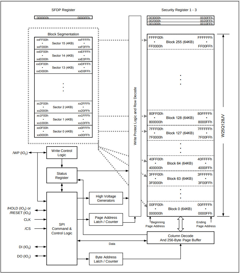
Во флеш-микросхеме байт является наименьшей единицей чтения и поддерживает произвольный доступ при чтении. Операции записи сложнее: чтобы записать 0, достаточно запрограммировать соответствующую ячейку хранения; но чтобы записать 1, необходимо сначала выполнить операцию стирания (erase). Из-за физических особенностей ячеек хранения флеш-памяти сектор является наименьшей единицей стирания, то есть нам нужно считать всё содержимое сектора, стереть этот сектор, а затем запрограммировать его согласно новым данным. Как видите, накладные расходы записи во флеш-память намного больше накладных расходов чтения.
Помимо массива хранения, флеш-микросхема также содержит несколько регистров, включая некоторые адресные регистры, используемые для управления адресом чтения/записи флеш-микросхемы, регистры управления, используемые для управления поведением микросхемы (такие как защита от записи, права доступа и т. д.), и регистры состояния, используемые для хранения текущего состояния чтения/записи флеш-микросхемы. Как видите, внутри флеш-микросхема по сути является контроллером устройства!
Чтобы обратиться к флеш-микросхеме, извне ей необходимо отправлять команды. Получив внешнюю команду, флеш-микросхема разбирает её (parse), а затем выполняет конкретную функцию, соответствующую команде. Это очень похоже на процесс выполнения инструкций CPU: цикл инструкции CPU включает выборку, декодирование, выполнение и обновление PC, тогда как для большинства устройств, включая флеш-микросхемы, процесс обработки включает приём команды, разбор, выполнение и ожидание новой команды. Что касается формата и функциональности команд, они, разумеется, определены соответствующим руководством. Например, 8-битная команда 03h означает чтение данных из флеш-микросхемы, и за командой следует 24-битный адрес ячейки хранения. Поэтому, если вы уже изучили проектирование CPU, вы вполне способны спроектировать основную логику флеш-микросхемы согласно её руководству.
С помощью шины мы можем легко преобразовывать запросы доступа к памяти со стороны CPU в команды чтения/записи для флеш-микросхемы. Возьмём в качестве примера запрос load, целевой адрес которого находится в пространстве флеш-памяти: когда LSU процессора выполняет инструкцию load, он инициирует на шине транзакцию чтения. Эта транзакция чтения проходит через Xbar и в конечном итоге достигает контроллера flash. Контроллер flash проверяет атрибуты транзакции, обнаруживает, что это транзакция чтения, затем генерирует соответствующую команду чтения, формирует адрес команды чтения на основе адреса в шинной транзакции и отправляет эту команду флеш-микросхеме. Через некоторое время контроллер flash получает данные, считанные из флеш-микросхемы, и передаёт их процессору в качестве ответа на шинную транзакцию. После того как LSU процессора получает результат чтения, выполнение инструкции load продолжается.
Используйте RTFSC, чтобы понять процесс чтения данных из flash
ysyxSoC содержит реализацию кода для описанного выше процесса и отображает пространство хранения flash на адресное пространство CPU 0x3000_0000~0x3fff_ffff. Вам нужно сначала обьявить (define) макрос FAST_FLASH в ysyxSoC/perip/spi/rtl/spi_top_apb.v, а затем попробовать разобраться в описанном выше процессе, сопоставляя его с кодом.
Что касается записи во flash, поскольку запись во flash требует сначала стереть весь сектор, а затем перезаписать весь набор данных, флеш-микросхеме необходимо отправить несколько команд. Однако в настоящий момент мы намерены использовать flash только для замены MROM, чтобы NPC мог выбирать корректные инструкции из flash после сброса. Поэтому пока мы не будем выполнять операции записи над флеш-микросхемой, и код флеш-микросхемы в ysyxSoC поддерживает только операции чтения.
Прочитайте данные из flash
Разобравшись в процессе чтения данных из flash, теперь вы можете протестировать этот процесс с помощью кода:
- Определите в среде моделирования массив, представляющий пространство хранения flash
- Запишите в этот массив некоторое содержимое при инициализации среды моделирования
- Эту операцию можно рассматривать как моделирование процесса прошивки данных во флеш-микросхему
- Корректно реализуйте функцию
flash_read(), чтобы она возвращала содержимое из соответствующего места flash в зависимости от параметраaddr - Напишите в
am-kernelsпростую тестовую программу, которая считывает содержимое из пространства хранения flash и проверяет его соответствие содержимому, установленному при инициализации среды моделирования
Доступ к флеш-микросхемам через шинный протокол SPI
Поскольку технологический процесс изготовления флеш-микросхем отличается от процесса изготовления процессоров, микросхему процессора и микросхему flash необходимо изготавливать раздельно, а затем припаивать на плату, где они взаимодействуют через дорожки платы. По этой причине важным фактором становится количество выводов (pins). С одной стороны, слишком большое число выводов затрудняет сохранение малого размера микросхемы, что негативно сказывается на компоновке и площади платы; с другой стороны, дорожки на плате обычно длиннее, чем внутри микросхемы, и сигналы более подвержены помехам, поэтому слишком большое число выводов также приводит к плотной трассировке на плате, а такие дорожки могут легко создавать взаимные помехи, влияя на стабильность сигнала.
Возьмём в качестве примера упомянутую выше команду чтения: одна операция чтения включает как минимум 8-битную команду, 24-битный адрес и 8-битные данные, что уже занимает 40 бит сигналов. Поэтому выводить все эти сигналы наружу флеш-микросхемы через выводы (pins) — не лучшее решение.
Чтобы сократить число выводов флеш-микросхемы, в неё обычно добавляют интерфейс шины SPI. SPI означает Serial Peripheral Interface («последовательный периферийный интерфейс») — это протокол последовательной шины, обеспечивающий связь между master и slave через несколько сигнальных линий.
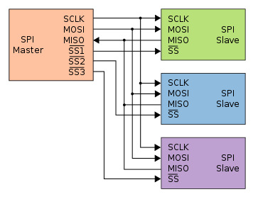
У шины SPI всего 4 вида сигналов:
SCK— тактовый сигнал, отправляемый master, всего 1 битSS— выбор slave (slave select), сигнал выбора, отправляемый master для указания цели взаимодействия; каждому slave соответствует 1 битMOSI— master output slave input, линия данных, по которой master передаёт данные slave, всего 1 битMISO— master input slave output, линия данных, по которой slave передаёт данные master, всего 1 бит
Чтобы взаимодействовать по шине SPI, master обычно сначала выбирает целевой slave с помощью сигнала SS, затем отправляет slave тактовые импульсы SPI через сигнал SCK, одновременно преобразуя отправляемую информацию в последовательный сигнал и передавая её slave побитово через сигнал MOSI; затем он отслеживает сигнал MISO и преобразует последовательный сигнал, полученный через MISO, обратно в параллельную информацию, тем самым получая ответ slave.
Slave работает аналогичным образом: если slave получает тактовые импульсы SCK, пока сигнал SS активен, он отслеживает сигнал MOSI и преобразует последовательный сигнал, полученный через MOSI, обратно в параллельную информацию, тем самым получая команду, отправленную master; после обработки команды он преобразует информацию ответа в последовательный сигнал и передаёт его master побитово через сигнал MISO.
Как видим, помимо конечного автомата, ядром реализации протокола шины SPI является преобразование между последовательными и параллельными сигналами, а именно то, как отправитель отправляет сигналы и как приёмник их сэмплирует и принимает. С одной стороны, необходимо учитывать порядок передачи (endianness): отправлять от старшего бита к младшему или наоборот; с другой стороны, необходимо учитывать момент отправки и сэмплирования (фазу тактового сигнала, clock phase): отправлять/сэмплировать по переднему или заднему фронту SCK. Иногда также согласуется уровень тактового сигнала в состоянии простоя (полярность тактового сигнала, clock polarity): простаивает ли он на высоком или низком уровне. В процессе отправки и сэмплирования SCK играет роль синхронизации: обе стороны совместно согласовывают порядок передачи и момент отправки/сэмплирования и корректно реализуют это соглашение на уровне RTL. В реальных сценариях у разных slave могут быть разные соглашения, а это значит, что при взаимодействии с разными slave master необходимо адаптировать свою отправку и сэмплирование под соглашение конкретного slave.
Однако программное обеспечение верхнего уровня не хочет заботиться об этом поведении на уровне сигналов, поэтому SPI master также должен абстрагировать это поведение на уровне сигналов в регистры устройства; программному обеспечению верхнего уровня достаточно обращаться к этим регистрам устройства, чтобы опрашивать или управлять SPI master. На самом деле, в архитектуре шины у SPI master двойная идентичность: с одной стороны, он является slave на шине AXI (или другом протоколе AMBA, например APB), отвечающим за приём команд от CPU; с другой стороны, он является master на стороне SPI, отвечающим за отправку команд SPI-устройствам slave. Поэтому мы также можем рассматривать SPI master как модуль-мост между AXI и SPI, используемый для преобразования запросов AXI в запросы SPI, тем самым обеспечивая взаимодействие со SPI-устройствами slave.
ysyxSoC интегрирует реализацию SPI master и отображает его регистры устройства на адресное пространство CPU 0x1000_1000~0x1000_1fff; соответствующий код и руководства находятся в соответствующих поддиректориях ysyxSoC/perip/spi/. Благодаря абстракции регистров устройства мы можем разобраться в поведении программного обеспечения верхнего уровня. Чтобы взаимодействовать с разными slave, master обычно должен поддерживать несколько соглашений, а какое соглашение использовать, настраивается через регистры устройства. Перед взаимодействием с slave драйвер SPI сначала устанавливает регистр SS, чтобы выбрать целевой slave, настраивает регистры управления SPI master согласно соглашению slave, затем записывает данные для передачи в регистр передаваемых данных и, наконец, записывает в регистр управления команду, означающую «начать передачу». Драйвер SPI может опрашивать регистр состояния SPI master: пока флаг состояния — «занято» (busy), он ждёт, и только когда флаг состояния становится «свободно» (idle), он может прочитать ответ slave из регистра принимаемых данных.
Реализуйте модуль разворота битов на основе протокола SPI
Чтобы освоиться с базовым процессом SPI и протестировать его, напишем простой модуль разворота битов, bitrev. Этот модуль принимает 8-битные входные данные и выводит результат разаорота битов этих данных, то есть меняет местами бит 0 с битом 7, бит 1 с битом 6 и так далее.
В частности, если вы выбираете Verilog, вам нужно реализовать соответствующий код в ysyxSoC/perip/bitrev/bitrev.v; если вы выбираете Chisel, вам нужно реализовать соответствующий код в модуле bitrevChisel файла ysyxSoC/src/device/BitRev.scala, а также изменить Module(new bitrev) в ysyxSoC/src/SoC.scala, чтобы создавать экземпляр модуля bitrevChisel.
Если бы входные и выходные сигналы этого модуля bitrev были 8-битными, это была бы простая комбинационная схема присваивания; но поскольку модуль bitrev взаимодействует через шину SPI, вам также нужно реализовать преобразование последовательных/параллельных сигналов (что тоже несложно — наш эталонный код на Chisel требует добавления всего 5 строк). Некоторые подсказки:
- Сигнал
SS, выводимый SPI master, активен по низкому уровню, и от slave требуется удерживать сигналMISOвысоким в состоянии простоя - Поскольку
SCKгенерирует импульсы только во время передач SPI, вам может понадобиться асинхронный сброс. Однако, поскольку этот модуль bitrev не участвует в tape-out, использование в нём асинхронного сброса не влияет на процесс tape-out- Если вы используете Chisel, вы можете обратиться к объяснению о Reset в документации Chisel
- Если вы используете Chisel и хотите срабатывать по заднему фронту тактового сигнала, вы можете обратиться к этому посту
- Вам также нужно отменить макрос
FAST_FLASH, обьявленный вysyxSoC/perip/spi/rtl/spi_top_apb.v, чтобы запросы APB могли обращаться к регистрам устройства SPI master
После реализации модуля bitrev в аппаратном обеспечении вам также нужно написать программу для его тестирования. Попробуйте написать программу AM, которая управляет SPI master для передачи 8-битных данных в модуль bitrev, а затем считывает обработанный результат и проверяет его соответствие ожиданиям. В частности:
- Установите данные для отправки в регистр TX SPI master
- Установите регистр делителя (divisor), который указывает отношение между частотой
SCKи текущей тактовой частотой SPI master во время передачи. Поскольку у verilator нет понятия частоты, вы можете установить делитель, обеспечивающий максимально высокую частотуSCK- В реальной микросхеме слишком высокая частота
SCKможет помешать slave работать корректно, поэтому регистр делителя необходимо устанавливать с учётом требований к рабочей частоте slave
- В реальной микросхеме слишком высокая частота
- Установите регистр
SS, чтобы выбрать модуль bitrev в качестве slave- ysyxSoC уже подключил bitrev в качестве SPI slave к SPI master, его номер slave — 7
- Установите регистр управления. В частности, вам нужно правильно установить каждое его поле; описания некоторых полей приведены ниже:
CHAR_LEN— поскольку длина как входных, так и выходных данных составляет 8 бит, длина передачи должна составлять 16 битRx_NEG,Tx_NEGиLSB— поскольку bitrev является лишь тестовым модулем и не участвует в финальном tape-out, мы не задаём эти детали для модуля bitrev; выбор соглашения оставлен на ваше усмотрение. Вам нужно выбрать соглашение, а затем реализовать модуль bitrev, настроить регистр управления SPI и написать программное обеспечение согласно этому соглашению, чтобы все три части могли взаимодействовать по одному и тому же соглашениюIE— пока мы не используем функцию прерыванийASS— устанавливать его или нет, решать вам, но это нужно учитывать вместе с программным обеспечением
- Опрашивайте флаг завершения в регистре управления, пока SPI master не завершит передачу данных
- Считайте данные, возвращённые slave, из регистра RX SPI master
Приведём пример одной передачи данных. Обратите внимание, что это лишь иллюстративная диаграмма, и ваша реализация не обязательно должна быть точно такой же:
                +---+   +---+   +---+   +---+   +---+   +---+   +---+   +---+   +---+   +---+   +---+   +---+   +---+   +---+   +---+   +---+
 SCK            |   |   |   |   |   |   |   |   |   |   |   |   |   |   |   |   |   |   |   |   |   |   |   |   |   |   |   |   |   |   |   |
        --------+   +---+   +---+   +---+   +---+   +---+   +---+   +---+   +---+   +---+   +---+   +---+   +---+   +---+   +---+   +---+   +------------
        --------+                                                                                                                               +--------
 SS             |                                                                                                                               |
                +-------------------------------------------------------------------------------------------------------------------------------+
        +-------+-------+-------+-------+-------+-------+-------+-------+-------+------------------------------------------------------------------------
MOSI            |   b7  |   b6  |   b5  |   b4  |   b3  |   b2  |   b1  |   b0  |
                +-------+-------+-------+-------+-------+-------+-------+-------+
        +-----------------------------------------------------------------------+-------+-------+-------+-------+-------+-------+-------+-------+--------
MISO                                                                            |   b0  |   b1  |   b2  |   b3  |   b4  |   b5  |   b6  |   b7  |
                                                                                +-------+-------+-------+-------+-------+-------+-------+-------+
Процесс передачи SPI включает множество деталей, и вам почти наверняка понадобятся RTFM и RTFSC, чтобы в них разобраться.
Прочитайте данные из flash через шину SPI
Попробуйте написать программу AM, реализующую функцию с прототипом uint32_t flash_read(uint32_t addr). Обратите внимание, что эта функция flash_read() отличается от одноимённой DPI-C-функции-интерфейса, упомянутой ранее. Эта функция flash_read() считывает 32-битное содержимое, начиная с адреса addr во флеш-микросхеме, управляя SPI master. Этот процесс похож на приведённый выше пример с bitrev:
- Установите команду, которую нужно отправить флеш-микросхеме, в регистр TX SPI master
- Установите регистр делителя
- Установите регистр
SS, чтобы выбрать флеш-микросхему в качестве slave; её номер slave — 0 - Установите регистр управления:
CHAR_LEN— поскольку команда чтения в сумме имеет длину 32 бита, а также нужно считать 32 бита данных, длина передачи должна составлять 64 битаRx_NEGиTx_NEG— необходимо установить согласно соответствующей документации slave- В реальной микросхеме неправильная установка
Rx_NEGиTx_NEGможет привести к нарушению времени удержания (hold time) во время работы схемы, из-за чего станет невозможно сэмплировать корректные данные. Однако у verilator нет понятия тайминга, поэтому некоторые некорректные настройки всё же могут давать верный результат; тем не менее мы всё равно рекомендуем сначала обратиться к официальному руководству (RTFM), а затем устанавливать их строго согласно соглашениям
- В реальной микросхеме неправильная установка
LSB— необходимо установить согласно соответствующей документации slave; при необходимости порядок байт считанных данных можно скорректировать программноIE— пока мы не используем функцию прерыванийASS— устанавливать его или нет, решать вам, но это нужно учитывать вместе с программным обеспечением
- Опрашивайте флаг завершения в регистре управления, пока SPI master не завершит передачу данных
- Считайте данные, возвращённые slave, из регистра RX SPI master
После реализации flash_read() используйте эту функцию, чтобы считать содержимое из пространства хранения flash, и проверьте его соответствие содержимому, установленному при инициализации среды моделирования.
Загрузите программу из flash и выполните её
Попробуйте сохранить упомянутую выше программу char-test во флеш-микросхему, напишите тестовую программу, которая с помощью flash_read() считывает char-test из flash по некоторому адресу в SRAM, а затем переходит по этому адресу для выполнения char-test.
Запрос инструкций из flash
После того как мы научились корректно читать данные из flash, мы можем рассмотреть возможность помещения выполняемой программы во flash и позволить NPC выбирать из flash свою первую инструкцию.
Постойте, что-то здесь не так... Мы только что читали содержимое из flash с помощью функции flash_read(). Эта функция также является частью программы; она компилируется в последовательность инструкций, размещаемую в MROM, а NPC выбирает и выполняет инструкции из MROM. Но если последовательность инструкций flash_read() тоже прошита во flash, кто будет выбирать и выполнять инструкции самой flash_read()? Это превращается в циклическую зависимость по принципу «курица или яйцо».
Если копнуть глубже, корень этой проблемы в том, что мы пытаемся реализовать запрос инструкций — поведение аппаратного уровня — с помощью программной функции. Это неразумно, поскольку запрос инструкций — это действие аппаратного уровня. Поэтому нам следует попытаться реализовать функциональность «запроса инструкций из flash» на аппаратном уровне.
Реализация функциональности flash_read() на аппаратном уровне означает обращение к регистрам SPI master в определённом порядке на аппаратном уровне. Возможно, вы уже догадались: реализовать функциональность flash_read() с помощью конечного автомата! В отличие от рассмотренного ранее подхода загрузки программы из flash с последующим её выполнением, такой способ выборки инструкций из флеш-микросхемы не требует предварительного чтения программы в память (упомянутую выше SRAM) перед выполнением, поэтому он также называется «выполнением на месте» (eXecute In Place, XIP).
Чтобы отличать это от обычного обращения к SPI master, нам нужно отобразить функциональность доступа к flash через XIP на адресное пространство, отличное от адресного пространства регистров устройства SPI master. На самом деле мы можем немного скорректировать ранее рассмотренное пространство хранения flash 0x3000_0000~0x3fff_ffff и определить его как пространство хранения flash, доступное через XIP. Xbar в ysyxSoC уже отобразил как адресное пространство SPI master 0x1000_1000~0x1000_1fff, так и пространство хранения flash 0x3000_0000~0x3fff_ffff на порт APB в модуле ysyxSoC/perip/spi/rtl/spi_top_apb.v, то есть порт APB в spi_top_apb.v может принимать запросы к обоим указанным выше диапазонам адресов, и вы можете различать их, проверяя целевой адрес запроса APB.
Обратитесь к flash через XIP
Подводя итог, общий процесс реализации XIP выглядит следующим образом:
- Проверьте целевой адрес запроса APB; если целевой адрес попадает в адресное пространство SPI master, обработайте его обычным образом и ответьте
- Если целевой адрес попадает в пространство хранения flash, войдите в режим XIP. В режиме XIP входные сигналы SPI master определяются соответствующим конечным автоматом
- Конечный автомат по очереди записывает соответствующие значения в регистры устройства SPI master; записываемые значения в целом такие же, как и в
flash_read() - Конечный автомат опрашивает флаг завершения SPI master и ожидает завершения передачи данных SPI master
- Конечный автомат считывает данные, возвращённые flash, из регистра RX SPI master, обрабатывает их и возвращает через APB, после чего выходит из режима XIP
- Конечный автомат по очереди записывает соответствующие значения в регистры устройства SPI master; записываемые значения в целом такие же, как и в
В частности, если вы выбираете Verilog, вам нужно реализовать соответствующий код в ysyxSoC/perip/spi/rtl/spi_top_apb.v; если вы выбираете Chisel, вам нужно реализовать соответствующий код в классе Impl файла ysyxSoC/src/device/SPI.scala.
Прежде чем выбирать инструкции через XIP, сначала протестируем, можно ли завершать через XIP запросы на чтение, выдаваемые CPU. Напишите тестовую программу, которая напрямую считывает содержимое из пространства хранения flash через указатель и проверяет его соответствие содержимому, установленному при инициализации среды моделирования.
Аналогично, в настоящее время мы не рассматриваем поддержку операций записи во flash через XIP, поэтому вам лучше найти способ сообщать об ошибке при обнаружении операции записи, чтобы своевременно диагностировать причину проблемы.
Выполните программу во flash через XIP
Сохраните упомянутую выше программу char-test во флеш-микросхему, напишите тестовую программу и перейдите во flash для выполнения char-test.
Замените MROM на flash
Убедившись, что инструкции могут выбираться и выполняться из flash, мы можем полностью заменить MROM на flash для хранения первой программы. Измените значение сброса PC так, чтобы NPC после сброса выбирал свою первую инструкцию из flash. Вам также нужно будет внести ряд других изменений для адаптации к этому переходу, включая... что ж, это остаётся вам самим разобраться, что также проверит, понимаете ли вы каждую деталь этого процесса.
Поскольку размер flash намного больше, чем ранее использовавшийся MROM, теперь мы можем хранить и выполнять более крупные программы; попробуйте запускать программы, включающие printf(), например coremark. Если вы запустите microbench, вы обнаружите, что немало подтестов не могут выполниться, поскольку область heap слишком мала.
coremark выполняется долго
Если бы вам разрешили вносить изменения, как бы вы сократили время выполнения coremark?
Подсказка: RTFSC
Попробуйте выполнить функцию flash_read() во flash
Вы можете обнаружить ошибки; попробуйте проанализировать, почему они возникают.
Добавьте CSR студенческого ID и выведите студенческий ID
Если вы уже реализовали ранее CSR студенческого ID, можете пропустить это задание.
Чтобы различать NPC разных студентов, вы можете задать собственный студенческий ID в идентификационных регистрах CSR. В частности, вы можете добавить в NPC следующие два CSR:
mvendorid— при чтении возвращает ASCII-код строкиysyx, то есть0x79737978marchid— при чтении возвращает десятичное представление числовой части студенческого ID; предположим, ваш студенческий ID —ysyx_22068888, тогда при чтении получается22068888, то есть0x150be98
После реализации вы можете считать значения двух указанных выше CSR и вывести их до того, как TRM riscv32e-ysyxsoc войдёт в функцию main().
Дождитесь завершения передачи SPI master через прерывания
Приведённая выше реализация XIP непрерывно опрашивает, завершена ли передача SPI master. На самом деле SPI master также поддерживает режим уведомления через прерывания: после установки бита IE в регистре управления SPI master будет генерировать сигнал прерывания по завершении передачи, и конечный автомат в режиме XIP может дожидаться завершения передачи SPI master, ожидая этот сигнал прерывания. Студенты, заинтересованные в этом, могут реализовать описанный выше подход ожидания на основе прерываний.
Хотя это не даёт заметного прироста производительности, в реальной системе реализация ожидания на основе прерываний может экономить энергию, поскольку запросы и ответы, выдаваемые при опросе (polling), не вносят реального вклада в работу системы.
Оперативная память с более высокой плотностью хранения
Решив проблему того, что MROM способна хранить лишь небольшие программы, с помощью flash, нам всё же необходимо рассмотреть хранение данных. Если программе нужно записать больше данных, чем предоставляемые SRAM 8 КБ, то она по-прежнему не сможет выполняться на ysyxSoC. Для этого нам нужна память большего объёма, которая также способна поддерживать выполнение процессором инструкций store.
Модуль хранения DRAM
DRAM (Dynamic Random Access Memory, динамическая оперативная память) — это широко используемый в настоящее время тип памяти. По сравнению с SRAM, DRAM обладает свойствами большой ёмкости и низкой стоимости. Ячейка хранения DRAM хранит 1 бит с помощью одного транзистора и одного конденсатора, где транзистор выполняет роль переключателя, функционально эквивалентного разрешению чтения/записи; конденсатор используется для хранения этого 1 бита информации. Когда заряд в конденсаторе превышает определённый порог, он считается 1, в противном случае — 0. Как видим, DRAM хранит информацию за счёт электрических свойств, поэтому является энергозависимой памятью; после отключения питания вся информация, хранящаяся в DRAM, теряется. И наоборот, при включении системы в DRAM также нет корректных данных.
Однако конденсаторы обладают свойством утечки заряда. Если ничего не предпринимать, заряд в конденсаторе будет постепенно уменьшаться, и в конце концов 1 превратится в 0, из-за чего станет невозможно определить, какие данные хранились изначально — 1 или 0, — что приведёт к потере данных. Чтобы избежать этой ситуации, ячейки хранения DRAM необходимо периодически обновлять (refresh): контроллер DRAM считывает информацию, хранящуюся в каждой ячейке хранения, и если это 1, перезаписывает эту ячейку хранения. Операция записи восстанавливает конденсатор ячейки хранения до состояния высокого заряда, так что в течение следующего периода времени из ячейки хранения снова можно будет считать 1, тем самым сохраняя хранимую информацию.
Как видим, запись в ячейку хранения DRAM по сути является зарядкой и разрядкой конденсатора. Поэтому, хотя операции записи DRAM не так быстры, как записи SRAM, с учётом таких факторов, как стоимость и ёмкость, операции записи DRAM всё же подходят для поддержки выполнения процессором инструкций store.
Если не учитывать организацию массива хранения и физический процесс чтения/записи, функционально микросхема DRAM очень похожа на рассмотренную ранее микросхему flash: помимо различных регистров, она также может принимать внешние команды для выполнения операций.
По аналогии с контроллером flash, модуль, отправляющий команды микросхеме DRAM для управления её работой, называется контроллером DRAM. Контроллер DRAM должен преобразовывать запросы шинных транзакций в команды для микросхемы DRAM и передавать эту информацию микросхеме DRAM через шину памяти. Кроме того, контроллеру DRAM также необходимо периодически отправлять микросхеме DRAM команды обновления (refresh). Однако это также увеличивает сложность проектирования контроллера DRAM: контроллер DRAM должен точно рассчитывать момент, когда требуется обновление: слишком частые операции обновления снижают эффективность выполнения команд чтения/записи, а слишком редкие операции обновления приводят к потере данных.
Микросхемы PSRAM
Существует тип микросхем DRAM со встроенной внутри логикой обновления (refresh), называемый микросхемами PSRAM (Pseudo Static Random Access Memory). Контроллеру PSRAM не нужно реализовывать функциональность обновления, а также не нужно заботиться о внутренней структуре микросхемы PSRAM, поэтому использование таких микросхем очень похоже на использование SRAM: достаточно предоставить адрес, данные и команду чтения/записи, чтобы обратиться к данным в микросхеме. Один из примеров — модель микросхемы PSRAM IS66WVS4M8ALL, предоставляющая 4 МБ пространства хранения; подробнее можно узнать из соответствующего руководства.
С помощью PSRAM мы можем попробовать предоставить программам в ysyxSoC более объёмную записываемую область памяти. По аналогии с доступом к флеш-микросхемам через протокол SPI, микросхемы PSRAM также предоставляют интерфейс SPI. Однако, в отличие от flash, PSRAM обычно выступает в роли оперативной памяти системы, поэтому необходимо обеспечить более эффективный способ доступа.
Доступ к микросхемам PSRAM через расширенную версию протокола шины SPI
На самом деле у протокола SPI есть несколько расширенных версий, способных повысить эффективность взаимодействия между master и slave. Базовый протокол SPI является дуплексным (full-duplex), то есть master и slave могут одновременно отправлять сообщения через MOSI и MISO соответственно. Но обычно master сначала отправляет команду slave, slave может обработать её только после получения, а затем отвечает master результатом обработки; для этого процесса достаточно полудуплексного (half-duplex) канала.
Протокол Dual SPI пользуется этим, используя одновременно MOSI и MISO базового протокола SPI для передачи в одном направлении, то есть протокол Dual SPI может передавать 2 бита в одном направлении в рамках одного такта SCK. Поскольку смысл MOSI и MISO изменился, в протоколе Dual SPI их названия меняются на SIO0 (Serial I/O 0) и SIO1 соответственно.
Чтобы отличать от способа передачи базового протокола SPI, slave обычно предоставляет разные команды, чтобы master мог выбрать, какой протокол использовать для передачи. Например, упомянутая выше модель флеш-микросхемы W25Q128JV предоставляет несколько команд чтения:
- Она предоставляет команду
03h, выполняющую операции чтения с использованием базового протокола SPI, где её команда, адрес и данные передаются по 1 биту. Обычно разрядность передачи этих трёх компонентов обозначается тройкой(разрядность передачи команды-разрядность передачи адреса-разрядность передачи данных). Например, базовый протокол SPI также обозначается как(1-1-1). Взяв в качестве примера чтение 32 бит данных, команде03hтребуется выполнить8 + 24 + 32 = 64тактовSCK. - Она также предоставляет команду
3Bh, выполняющую операции чтения с использованием протокола Dual SPI; её команда и адрес передаются по 1 биту, но данные передаются по 2 бита, что обозначается как(1-1-2). Взяв в качестве примера чтение 32 бит данных, команде3Bhтребуется выполнить8 + 24 + 32/2 = 48тактовSCK. Однако, независимо от того, по сколько бит передаются данные, чтение данных из массива хранения flash всегда занимает определённую задержку, поэтому команде3Bhтакже требуется дополнительно подождать 8 тактовSCKперед передачей данных, то есть команде3Bhтребуется выполнить8 + 24 + 8 (задержка чтения) + 32/2 = 56тактовSCK. - Она также предоставляет команду
BBh, выполняющую операции чтения с использованием протокола Dual SPI; её команда передаётся по 1 биту, но адрес и данные передаются по 2 бита, что обозначается как(1-2-2). Взяв в качестве примера чтение 32 бит данных, командеBBhтребуется выполнить8 + 24/2 + 4 (задержка чтения) + 32/2 = 40тактовSCK.
Кроме того, существует протокол Quad SPI (сокращённо QSPI), добавляющий два новых сигнала, SIO2 и SIO3, что позволяет передавать 4 бита в одном направлении в рамках одного такта SCK. Например, упомянутая выше модель флеш-микросхемы W25Q128JV также предоставляет ещё две команды чтения на основе протокола QSPI:
- Она предоставляет команду
6Bh, где её команда и адрес передаются по 1 биту, но данные передаются по 4 бита, что обозначается как(1-1-4). Взяв в качестве примера чтение 32 бит данных, команде6Bhтребуется выполнить8 + 24 + 8 (задержка чтения) + 32/4 = 48тактовSCK. - Она также предоставляет команду
EBh, где её команда передаётся по 1 биту, но адрес и данные передаются по 4 бита, что обозначается как(1-4-4). Взяв в качестве примера чтение 32 бит данных, командеEBhтребуется выполнить8 + 24/4 + 6 (задержка чтения) + 32/4 = 28тактовSCK.
Однако в приведённых выше командах чтения, независимо от того, по сколько бит передаются части адреса и данных, часть команды всегда передаётся по 1 биту. Это потому, что slave узнаёт, какой протокол следует использовать для передачи последующих адреса и данных, только после разбора команды, поэтому часть команды по-прежнему следует базовому протоколу SPI и передаётся побитово. Кроме того, хотя упомянутая выше модель флеш-микросхемы поддерживает несколько способов передачи, SPI master, подключённый к флеш-микросхеме, может передавать данные только с использованием базового протокола SPI, поэтому он не может выдавать другие команды чтения.
ysyxSoC интегрирует реализацию контроллера PSRAM и отображает пространство хранения PSRAM на адресное пространство CPU 0x8000_0000~0x9fff_ffff. Код контроллера PSRAM расположен в директории ysyxSoC/perip/psram/efabless/ и использует протокол шины wishbone. Мы инкапсулировали его в протокол шины APB (см. ysyxSoC/perip/psram/psram_top_apb.v) и подключили в APB Xbar ysyxSoC. Контроллер PSRAM преобразует полученные шинные транзакции в команды, отправляемые микросхеме PSRAM. Мы выбрали для моделирования модель микросхемы PSRAM IS66WVS4M8ALL, которая поддерживает протокол QSPI, поэтому контроллер PSRAM, интегрированный в ysyxSoC, может взаимодействовать с микросхемой PSRAM через протокол QSPI, что позволяет использовать более эффективные команды для доступа к PSRAM. ysyxSoC уже подключил микросхему PSRAM к контроллеру PSRAM, но не предоставляет код для самой микросхемы PSRAM. Чтобы использовать PSRAM в ysyxSoC, вам всё же нужно реализовать поведенческую модель микросхемы PSRAM.
Реализуйте поведенческую модель микросхемы PSRAM для моделирования
Вам нужно реализовать поведенческую модель микросхемы IS66WVS4M8ALL. Вам достаточно реализовать только две команды в режиме SPI Mode — Quad IO Read и Quad IO Write, чьи кодировки команд — EBh и 38h соответственно; контроллер PSRAM будет отправлять микросхеме PSRAM только эти две команды.
В частности, если вы выбираете Verilog, вам нужно реализовать соответствующий код в ysyxSoC/perip/psram/psram.v; если вы выбираете Chisel, вам нужно реализовать соответствующий код в модуле psramChisel файла ysyxSoC/src/device/PSRAM.scala, а также изменить Module(new psram) в ysyxSoC/src/SoC.scala, чтобы создавать экземпляр модуля psramChisel.
Некоторые пояснения:
- Смысл порта
ce_nтакой же, как уSSв протоколе шины SPI; он активен по низкому уровню - Порт
dioобъявлен как типinoutи вместе с сигналом разрешения вывода (output enable) может реализовывать трёхстабильную логику (tri-state logic), которая может одновременно использоваться для входа или выхода, обеспечивая полудуплексную передачу сигналов- В маршруте ASIC ячейку трёхстабильной логики из библиотеки стандартных ячеек необходимо явно создавать как экземпляр, но здесь мы только тестируем в среде моделирования, поэтому нет необходимости обращаться к библиотеке стандартных ячеек
- Если вы используете Verilog, вы можете обратиться к соответствующему коду
qspi_dioвysyxSoC/perip/psram/psram_top_apb.v - Если вы используете Chisel, поскольку Chisel в настоящее время не поддерживает операции над типом
Analog, кроме соединений, мы уже создали в каркасном коде подмодульTriStateBuf, который разбиваетdioнаdinиdout— сигналы типаUIntв двух направлениях — для последующего использования
- Массив хранения достаточно реализовать как двумерный массив со словом длиной 8 бит; не нужно заботиться о его физической организации, основное внимание следует уделить протоколу QSPI. Кроме того, поскольку PSRAM не является энергонезависимой памятью, нет необходимости устанавливать её содержимое при инициализации среды моделирования, поэтому вы можете напрямую определить массив хранения в коде на Verilog либо обращаться к массиву, определённому в коде на C++, через DPI-C, что удобно для трассировки с помощью mtrace
- В руководстве также есть режим QPI Mode, смысл которого отличается от упомянутого выше QSPI, и его пока можно игнорировать
- Для таких деталей, как порядок байт и фаза тактового сигнала, вы можете обратиться к официальному руководству (RTFM), используя соответствующее руководство, либо к RTFSC, используя код контроллера PSRAM
- Для корректной реализации взаимодействия между контроллером PSRAM и микросхемой PSRAM вам не нужно изменять код контроллера PSRAM
После реализации протестируйте небольшой участок доступа к PSRAM (например, 4 КБ) с помощью mem-test, чтобы проверить корректность вашей реализации. Обратите внимание, что flash теперь предоставляет более объёмное пространство хранения для программ, поэтому вы можете вызывать printf() в mem-test, чтобы выводить отладочную информацию, особенно информацию, связанную с ходом теста, чтобы вы могли знать, нормально ли протекает тест.
На самом деле поверх QSPI существует протокол под названием QPI, способный дополнительно повысить эффективность передачи части команды, то есть команда, адрес и данные все передаются по 4 бита, что обозначается как (4-4-4). Однако для совместимости со старыми SPI master slave обычно при включении питания находится в базовом режиме SPI, взаимодействуя в этот момент через базовый протокол SPI. Если slave поддерживает протокол QPI, он предоставит команду для переключения в режим QPI; master может отправить эту команду, чтобы переключить slave в режим QPI, а затем взаимодействовать с ним, используя протокол QPI.
Используйте протокол QPI для доступа к микросхеме PSRAM
Попробуйте добавить в микросхему PSRAM режим QPI и команду для входа в режим QPI, затем измените код контроллера PSRAM так, чтобы после сброса он сначала отправлял микросхеме PSRAM команду входа в режим QPI посредством схемной логики, а затем взаимодействовал с микросхемой PSRAM в режиме QPI.
Обратите внимание, что добавление этой функциональности прозрачно для программного обеспечения верхнего уровня; программное обеспечение верхнего уровня может повысить эффективность доступа к PSRAM без каких-либо изменений.
Выполнение более крупных программ
С поддержкой PSRAM мы можем попробовать разместить сегмент данных в PSRAM, тем самым поддержав выполнение более крупных программ.
Запустите microbench на ysyxSoC
Ранее мы размещали сегмент данных и область heap в 8 КБ SRAM, а для выполнения microbench требуется более 8 КБ памяти, поэтому немало подтестов не могли выполниться. После размещения сегмента данных и области heap в 4 МБ PSRAM вы должны увидеть, что microbench успешно проходит все тесты в масштабе test.
Мы только что запустили microbench, что лишь демонстрирует с точки зрения процесса, что размещение сегмента данных в PSRAM работает нормально; но прежде чем запускать больше программ, нам следует сначала полностью протестировать 4 МБ PSRAM с помощью mem-test. Однако полное тестирование чтения/записи этого 4 МБ пространства хранения с помощью mem-test в среде моделирования заняло бы очень много времени.
Это происходит потому, что в настоящее время мы выполняем mem-test во flash: для выборки одной инструкции из flash требуется как минимум 64 такта SCK; а поскольку SPI master генерирует тактовый сигнал SCK путём деления частоты, даже при наиболее эффективном делении на 2, сам процесс передачи SPI занимает как минимум 128 тактов CPU; добавив накладные расходы на управление конечным автоматом XIP, выборка одной инструкции из flash в сумме занимает около 150 тактов CPU.
Из-за наличия циклов и вызовов функций большая часть кода в программе выполняется многократно. По сравнению с тем, чтобы позволять программе продолжать выполняться во flash, потратив немного времени заранее на загрузку кода в память с более высокой эффективностью доступа, чем flash, а затем позволив программе многократно выполняться в этой памяти, можно эффективно повысить эффективность выполнения программы. Однако этот процесс загрузки требует считать инструкции программы, а затем записать их в целевую память, поэтому необходима память, поддерживающая операции записи. PSRAM пока ещё находится на стадии тестирования; учитывая, что mem-test не очень велика, мы можем попробовать загрузить mem-test в упомянутую выше SRAM объёмом 8 КБ.
Кто выполняет эту операцию загрузки? Нам, безусловно, нужно завершить загрузку до того, как начнёт выполняться mem-test, но мы также хотим сохранить особенность «выборки инструкций из flash после сброса NPC», чтобы среда моделирования не вмешивалась слишком сильно, а операция загрузки могла бы также выполняться на реальной микросхеме. Поэтому нам нужно использовать промежуток между сбросом NPC и фактическим выполнением mem-test для выполнения загрузки, и нетрудно догадаться — это же bootloader! Иными словами, нам нужно расширить функциональность bootloader'а, чтобы он загружал весь код и данные программы в SRAM, а затем переходил в SRAM для выполнения.
Полностью протестируйте доступ к PSRAM
Расширьте функциональность bootloader'а так, чтобы он полностью загружал mem-test в SRAM, а затем выполнял mem-test. Некоторые подсказки:
- Вам также нужно загрузить сегмент данных, доступных только для чтения, в SRAM вместе с остальными данными; он может содержать некоторые данные, необходимые во время выполнения кода, например таблицы переходов
- Если вы обнаружите, что код
mem-testслишком велик, чтобы поместиться в SRAM, попробуйте использовать опцию компиляции-Os, чтобы указать gcc оптимизировать по размеру кода - Реализация загрузки кода также требует обработки нескольких деталей, которые вы уже способны понять на данном этапе; если вы их проигнорируете, то узнаете о них через отладку, поскольку реальные проекты в будущем будут выглядеть именно так
После этого позвольте mem-test протестировать все 4 МБ пространства хранения в PSRAM; вы обнаружите, что эффективность выполнения mem-test значительно возросла, и тест можно завершить примерно за 10 минут.
Хотя доступ к SRAM быстрый, её ёмкость мала и не может вместить большинство программ. Полностью протестировав доступ к PSRAM, мы также можем рассмотреть возможность того, чтобы bootloader полностью загружал программу в PSRAM, тем самым повышая эффективность выполнения программы.
Загрузите программу в PSRAM через bootloader для выполнения
Вы уже загружали mem-test в SRAM через bootloader, поэтому загрузка программы в PSRAM не составит труда. Однако, чтобы полностью использовать SRAM, мы можем разместить стек в SRAM, чтобы повысить эффективность вызовов функций и доступа к локальным переменным.
Попробуйте выполнить microbench в масштабе test; вы обнаружите, что по сравнению с выполнением во flash, загрузка в PSRAM и выполнение там даёт значительный прирост производительности.
Выполните RT-Thread на PSRAM
Ёмкости PSRAM теперь достаточно для запуска RT-Thread. Попробуйте загрузить RT-Thread в PSRAM через bootloader для выполнения.
Если программа велика, процесс загрузки программы bootloader'ом также займёт больше времени, поскольку сам bootloader выполняется во flash. Аналогично, можем ли мы сначала загрузить код «bootloader загружает программу» в память с более высокой эффективностью доступа, а затем выполнить функциональность «bootloader загружает программу»? На самом деле это многоэтапный процесс загрузки bootloader'а. Для удобства различения мы можем разделить всю работу bootloader'а на две части: FSBL (first stage bootloader, загрузчик первого этапа) и SSBL (second stage bootloader, загрузчик второго этапа). При включении системы FSBL, SSBL и выполняемая программа все находятся во flash; первым выполняется FSBL, который отвечает за загрузку SSBL из flash в другую память, а затем переход на SSBL; далее SSBL отвечает за загрузку следующей выполняемой программы из flash в PSRAM, а затем переход на программу и её выполнение. На самом деле код SSBL невелик, поэтому мы можем сделать так, чтобы FSBL загружал SSBL в SRAM для выполнения, что ускорит выполнение SSBL.
Реализуйте двухэтапный процесс загрузки bootloader'а
Реализуйте FSBL и SSBL согласно описанной выше функциональности. Чтобы знать диапазон SSBL во flash, вам может понадобиться разместить SSBL в отдельной секции; подробности можно найти в соответствующем коде start.S.
Кроме того, поскольку bootloader разбивает работу по загрузке на несколько этапов, вам также нужно учитывать, доступен ли целевой объект на текущем этапе.
Внутренняя структура микросхем SDRAM
Если мы хотим ещё больше повысить эффективность доступа к микросхемам DRAM, нам нужно рассмотреть замену последовательной шины между контроллером и микросхемой на параллельную шину. Например, внутренняя структура модели микросхемы DRAM MT48LC16M16A2 показана на рисунке ниже. У этой микросхемы 39 выводов, включая:
CLK,CKE— тактовый сигнал и сигнал разрешения тактированияCS#,WE#,CAS#,#RAS— командные сигналыBA[1:0]— адрес банка (bank)A[12:0]— адресDQ[15:0]— данныеDQM[1:0]— маска данных, на рисунке ниже обозначена какDQMLиDQMH
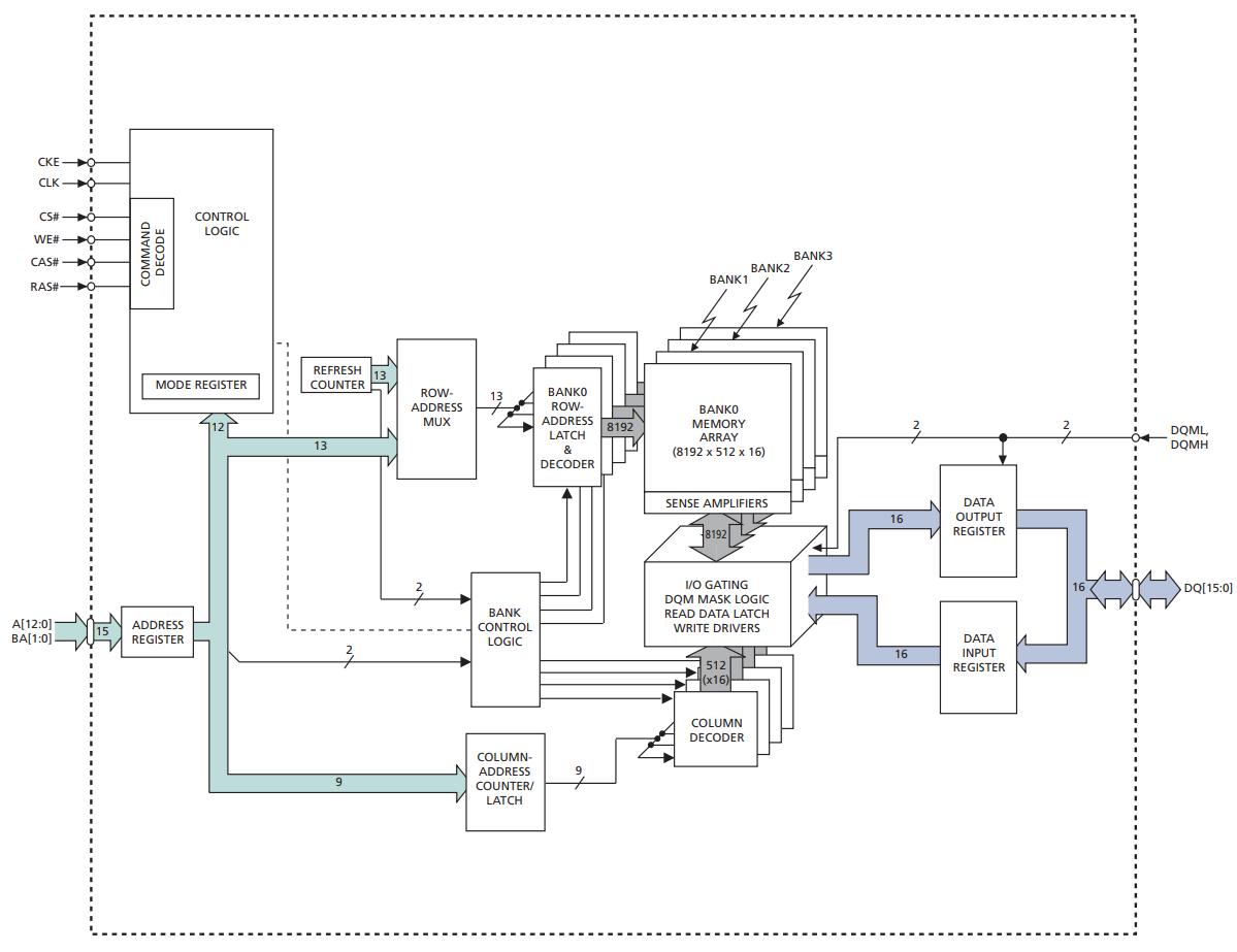
В отличие от делённого по частоте SCK в протоколе SPI, тактовый сигнал CLK здесь обычно управляется непосредственно тактовым сигналом контроллера DRAM. Такой тип DRAM называется синхронной DRAM, то есть SDRAM (Synchronous Dynamic Random Access Memory). Микросхемы SDRAM стали сегодня основным типом микросхем памяти; самая ранняя коммерчески доступная микросхема SDRAM была выпущена в 1992 году и относилась к SDR SDRAM (Single Data Rate SDRAM), передающей данные один раз за такт. Модель микросхемы MT48LC16M16A2, показанная на рисунке выше, относится к микросхемам SDR SDRAM. Начиная с 1997 года появилась DDR SDRAM (Double Data Rate SDRAM), способная передавать данные как по переднему, так и по заднему фронту тактового сигнала, тем самым увеличивая пропускную способность передачи данных; впоследствии одна за другой появились DDR2, DDR3, DDR4 и DDR5, каждая из которых за счёт разных технологий ещё больше увеличивала пропускную способность передачи данных. В противовес синхронной DRAM существует также асинхронная DRAM, чьи шинные сигналы не включают тактовый сигнал. В настоящее время асинхронная DRAM практически полностью вытеснена SDRAM, поэтому сегодня, говоря о DRAM, почти всегда имеют в виду SDRAM.
В отличие от интерфейса шины SPI микросхемы PSRAM, выводы традиционной микросхемы DRAM включают такую информацию, как адрес банка, что требует от контроллера DRAM понимания внутренней организации массива хранения в микросхеме DRAM, чтобы знать, какую информацию выводить на связанные с адресом выводы.
Массив хранения микросхемы DRAM имеет многомерную структуру, логически состоящую из нескольких матриц, где одна матрица также называется банком памяти (memory bank). Элемент матрицы в банке памяти состоит из нескольких ячеек хранения, и каждая ячейка хранения содержит один транзистор и один конденсатор, используемые для хранения 1 бита информации. Элемент матрицы в банке памяти должен указываться совместно адресом строки и адресом столбца. Например, у указанной выше микросхемы DRAM 4 банка памяти, каждый с 8192 строками и 512 столбцами, а элемент матрицы в банке памяти содержит 16 ячеек хранения, поэтому ёмкость этой микросхемы DRAM составляет 4 * 8192 * 512 * 16 = 256 Мбит = 32 МБ.
При чтении сначала выбирается целевой банк памяти по номеру банка. Затем активируется строка в целевом банке памяти через адрес строки: усилитель считывания (sense amplifier) в целевом банке памяти обнаруживает заряды во всех ячейках хранения этой строки, тем самым узнавая, хранит ли каждая ячейка хранения 1 или 0. Усилитель считывания в основном состоит из пары перекрёстно связанных инверторов, поэтому он способен хранить информацию; отсюда усилитель считывания в банке памяти также называется буфером строки (row buffer), способным хранить одну строку информации. После этого согласно адресу столбца данные выбираются из буфера строки целевого банка памяти и выводятся наружу микросхемы DRAM в качестве результата чтения. При записи сначала записываемые данные записываются в соответствующие позиции буфера строки, а затем заряжаются или разряжаются конденсаторы соответствующих ячеек хранения, тем самым перенося содержимое буфера строки в ячейки хранения. Если требуется обратиться к другой строке данных, перед активацией другой строки информацию текущей активированной строки необходимо сначала записать обратно в ячейки хранения; этот процесс называется предзарядом (precharge).
Физическая реализация микросхем DRAM
Учитывая ограничения физической реализации, чрезмерно длинные дорожки вносят большие задержки. Поэтому с точки зрения физической реализации банк памяти микросхемы DRAM дополнительно разбивается на несколько подмассивов (subarray). Однако структура и способ доступа к этим подмассивам прозрачны для внешней стороны микросхемы, и контроллеру DRAM не нужно заботиться о них при отправке команд микросхеме DRAM. Заинтересованные студенты могут прочитать эту статью, чтобы глубже понять физическую структуру внутри микросхемы DRAM.
Разобравшись во внутренней организации микросхем DRAM, мы можем систематизировать команды микросхем DRAM. Команды разных версий SDRAM немного отличаются; в следующей таблице перечислены команды SDR SDRAM:
| CS# | RAS# | CAS# | WE# | Команда | Значение |
|---|---|---|---|---|---|
| 1 | X | X | X | COMMAND INHIBIT | Нет команды |
| 0 | 1 | 1 | 1 | NO OPERATION | NOP |
| 0 | 0 | 1 | 1 | ACTIVE | Активировать строку в целевом банке памяти |
| 0 | 1 | 0 | 1 | READ | Прочитать столбец из целевого банка памяти |
| 0 | 1 | 0 | 0 | WRITE | Записать столбец в целевой банк памяти |
| 0 | 1 | 1 | 0 | BURST TERMINATE | Остановить текущую пакетную передачу |
| 0 | 0 | 1 | 0 | PRECHARGE | Закрыть активированную строку в банке памяти (предзаряд) |
| 0 | 0 | 0 | 1 | AUTO REFRESH | Обновление |
| 0 | 0 | 0 | 0 | LOAD MODE REGISTER | Установить регистр Mode |
Приведённые выше команды затрагивают понятие «пакетной передачи» (burst transfer), которая означает транзакцию, содержащую несколько последовательных передач данных, где одна передача данных называется «тактом передачи» (beat). Возьмём в качестве примера чтение: от момента получения микросхемой DRAM команды READ до момента считывания данных из массива хранения и передачи их на шину DQ обычно требуется несколько тактов, и эта задержка называется задержкой CAS (CAS latency, в некоторых учебниках переводится как «период задержки CAS»). Взяв в качестве примера указанную выше модель MT48LC16M16A2, в зависимости от рабочей частоты, задержка CAS может составлять от 1 до 3 тактов, то есть от получения команды READ до считывания 16 бит данных на шину DQ проходит задержка от 1 до 3 тактов. Предположим, что задержка CAS составляет 2 такта: если не использовать пакетную передачу, для считывания 8 байт нужно отправить команду READ 4 раза, всего 12 тактов; если использовать пакетную передачу, достаточно отправить всего 1 команду READ, что обойдётся в 6 тактов.
// normal
  1   1   1   1   1   1   1   1   1   1   1   1
|---|---|---|---|---|---|---|---|---|---|---|---|
  ^       |   ^       |   ^       |   ^       |
  |       v   |       v   |       v   |       v
 READ   data READ   data READ   data READ   data

// burst
  1   1   1   1   1   1
|---|---|---|---|---|---|
  ^       |   |   |   |
  |       v   v   v   v
 READ    1st 2nd 3rd 4th
Команда WRITE также поддерживает пакетную передачу, то есть для записи 8 байт данные для записи можно передавать непрерывно в 3 такта, следующих сразу за выдачей команды WRITE. Что касается того, сколько тактов передачи содержит транзакция пакетной передачи, это можно настроить через регистр Mode. Регистр Mode также может настраивать такие параметры, как задержка CAS.
ysyxSoC интегрирует реализацию контроллера SDR SDRAM (далее именуемого контроллером SDRAM) и отображает пространство хранения SDRAM на адресное пространство CPU 0xa000_0000~0xbfff_ffff. Код контроллера SDRAM расположен в директории ysyxSoC/perip/sdram/core_sdram_axi4/ и использует протокол шины AXI4. Для удобства раннего тестирования мы инкапсулировали его основную часть ysyxSoC/perip/sdram/core_sdram_axi4/sdram_axi4_core.v в протокол шины APB (см. ysyxSoC/perip/sdram/sdram_top_apb.v) и подключили в APB Xbar ysyxSoC. Контроллер SDRAM преобразует полученные шинные транзакции в команды, отправляемые микросхеме SDRAM. Мы выбрали для моделирования модель микросхемы SDRAM MT48LC16M16A2. ysyxSoC уже подключил микросхему SDRAM к контроллеру SDRAM, но не предоставляет код для самой микросхемы SDRAM. Чтобы использовать SDRAM в ysyxSoC, вам всё же нужно реализовать поведенческую модель микросхемы SDRAM.
Реализуйте поведенческую модель микросхемы SDRAM для моделирования
Вам нужно реализовать поведенческую модель микросхемы MT48LC16M16A2. В частности, вам нужно реализовать команды, которые будет отправлять контроллер SDRAM, среди которых команды PRECHARGE и AUTO REFRESH связаны с электрическими характеристиками ячеек хранения и не нужны в среде моделирования, поэтому их можно реализовать как NOP. Кроме того, для регистра Mode достаточно реализовать только CAS Latency и Burst Length; остальные поля можно игнорировать.
В частности, если вы выбираете Verilog, вам нужно реализовать соответствующий код в ysyxSoC/perip/sdram/sdram.v; если вы выбираете Chisel, вам нужно реализовать соответствующий код в модуле sdramChisel файла ysyxSoC/src/device/SDRAM.scala, а также изменить Module(new sdram) в ysyxSoC/src/SoC.scala, чтобы создавать экземпляр модуля sdramChisel.
Что касается остальных деталей, обратитесь к официальному руководству (RTFM), используя соответствующее руководство, либо к RTFSC, используя код контроллера SDRAM. Для корректной реализации взаимодействия между контроллером SDRAM и микросхемой SDRAM вам не нужно изменять код контроллера SDRAM.
После реализации протестируйте небольшой участок доступа к SDRAM (например, 4 КБ) с помощью mem-test, чтобы проверить корректность вашей реализации.
Полностью протестируйте доступ к SDRAM
Прежде чем загружать программы в SDRAM для выполнения, сначала полностью протестируем доступ ко всему пространству хранения указанной выше микросхемы SDRAM с помощью mem-test. Завершение этого теста занимает около 1 часа.
Загрузите программу в SDRAM для выполнения
Позвольте bootloader'у загрузить программу в SDRAM и выполнить её. После этого попробуйте выполнить microbench и RT-Thread на SDRAM.
Расширение микросхем SDRAM
Как упоминалось выше, ёмкость микросхемы SDR SDRAM MT48LC16M16A2 составляет 32 МБ. Но сегодняшние модули памяти часто достигают 4 ГБ; как это достигается? Хотя современные основные модули памяти используют более совершенные технологические процессы, и ёмкость одной микросхемы памяти выросла, 4 ГБ всё же не достигается только за счёт одной микросхемы памяти. На самом деле это достигается путём объединения и расширения нескольких микросхем памяти по определённым измерениям. Если вы наблюдали структуру модуля памяти, вы заметите, что на одном модуле памяти расположено несколько микросхем памяти, а сам модуль памяти представляет собой особую печатную плату (PCB): он интегрирует несколько микросхем памяти со стандартными размерами и использует интерфейс DIMM, что позволяет вставлять его в слоты памяти материнской платы.
Мы знаем, что без учёта физической организации память представляет собой двумерную матрицу, где каждая строка хранит одно слово, а номер строки является адресом. С этой точки зрения расширение с помощью нескольких микросхем — это не что иное, как расширение по двум измерениям: одно измерение — хранить больше бит информации по одному адресу, называемое битовым расширением (bit extension); другое измерение — увеличивать диапазон адресов, называемое словарным расширением (word extension).
Идея битового расширения состоит в том, что разные микросхемы одновременно считывают данные по одному и тому же адресу, что не только увеличивает ёмкость памяти, но и повышает пропускную способность доступа к памяти. Если длина слова микросхемы (то есть разрядность сигнала DQ) меньше разрядности данных шины, битовое расширение может значительно повысить эффективность передачи данных. Например, для 64-битного CPU разрядность данных шины обычно не менее 64 бит; используя 4 микросхемы MT48LC16M16A2 с длиной слова 16 бит, можно считать 64 бита после одной задержки CAS, что даже эффективнее пакетной передачи:
  1   1   1
|---|---|---|
  ^       |
  |       v
 READ   data[15:0]  (chip0)

  1   1   1
|---|---|---|
  ^       |
  |       v
 READ   data[31:16] (chip1)

  1   1   1
|---|---|---|
  ^       |
  |       v
 READ   data[47:32] (chip2)

  1   1   1
|---|---|---|
  ^       |
  |       v
 READ   data[63:48] (chip3)
Другой пример — модель модуля памяти DDR4 SDRAM MTA9ASF51272PZ. Длина слова микросхем на этом модуле составляет 8 бит, но за счёт битового расширения с 8 микросхемами можно за раз считывать и записывать 64 бита.
Расширьте разрядность данных контроллера SDRAM до 32 бит
Создайте экземпляры подмодулей 2 микросхем SDRAM, чтобы смоделировать сценарий битового расширения 2 микросхем SDRAM. Для этого вам нужно изменить следующее:
- Разрядность некоторых сигналов в интерфейсе шины SDRAM
- Если вы используете Chisel, вы можете напрямую изменить определение
SDRAMIO - Если вы используете Verilog
- Если вы не планируете участвовать в tape-out, вы можете напрямую изменить соответствующую разрядность сигналов в
ysyxSoC/build/ysyxSoCFull.v - Если вы планируете участвовать в tape-out, вы не можете напрямую изменять
ysyxSoC/build/ysyxSoCFull.v, иначе автоматизированный процесс тестирования для tape-out перезапишет ваши изменения вysyxSoC/build/ysyxSoCFull.v; вместо этого вы можете добавить несколько команд вysyxSoC/Makefile, которые смогут автоматически изменять разрядность сигналов после генерацииysyxSoC/build/ysyxSoCFull.v
- Если вы не планируете участвовать в tape-out, вы можете напрямую изменить соответствующую разрядность сигналов в
- Если вы используете Chisel, вы можете напрямую изменить определение
- Внутреннюю реализацию контроллера SDRAM
После реализации битового расширения больше не нужно обращаться к микросхемам SDRAM через режим пакетной передачи; после одной задержки CAS из расширенных микросхем можно считать 32 бита данных. Попробуйте запустить несколько бенчмарков, чтобы сравнить изменения производительности до и после битового расширения.
Однако этот прирост производительности не даётся бесплатно. Битовое расширение требует линейного роста числа выводов DQ, что требует тщательного расчёта для микросхем, заботящихся о стоимости. Кроме того, даже если стоимость не является проблемой, прирост производительности от битового расширения также ограничен другими факторами системы, такими как разрядность данных шины: если одна передача по шине может составлять максимум 64 бита, то даже если длина слова микросхем памяти будет расширена до 512 бит, значимого общего выигрыша не будет получено — точно так же, как поток в водопроводной трубе ограничен её самым узким участком.
Другое измерение — словарное расширение, идея которого заключается в распределении разных адресов по разным микросхемам, тем самым увеличивая ёмкость доступа к памяти. Например, мы можем использовать 2 микросхемы MT48LC16M16A2 по 32 МБ, чтобы через словарное расширение сформировать память ёмкостью 64 МБ. Указанное выше словарное расширение требует добавления всего 1 бита адреса на шине памяти, и рост числа выводов имеет логарифмическую зависимость от ёмкости хранения, поэтому накладные расходы невелики по сравнению с битовым расширением. Но интуитивно словарное расширение не может напрямую повысить пропускную способность доступа к памяти; мы продолжим обсуждать эту проблему в следующих разделах.
Словарное расширение для контроллера SDRAM
Создайте экземпляры в общей сложности 4 микросхем SDRAM, где между двумя парами микросхем SDRAM выполняется битовое расширение, а затем над результатами битового расширения выполняется словарное расширение. Вам также нужно изменить интерфейс шины SDRAM и внутреннюю реализацию контроллера.
После реализации протестируйте всё расширенное пространство хранения с помощью mem-test. Завершение этого теста занимает несколько часов.
Обратите внимание, что ваши изменения могут привести к тому, что контроллер SDRAM перестанет удовлетворять электрическим характеристикам микросхем SDRAM, из-за чего он не сможет работать с реальными микросхемами SDRAM. Однако тестирование электрических характеристик SDRAM требует более сложной среды моделирования. Чтобы не усложнять задачу, мы не требуем, чтобы изменённый контроллер SDRAM корректно работал на реальной плате.
Доступ к большему числу периферийных устройств
Вся работа выше велась вокруг TRM. Наконец, посмотрим, как поддержать IOE.
GPIO
Сначала добавим поддержку GPIO. GPIO, пожалуй, простейшая периферия; по сути это провод, соединяющий внутреннюю и внешнюю части микросхемы, и, очевидно, он должен занимать выводы микросхемы. Через GPIO микросхема может напрямую выводить внутренние сигналы наружу микросхемы, чтобы управлять некоторыми простыми устройствами, например светодиодами на плате; микросхема также может получать через GPIO некоторые простые внешние состояния, например состояния DIP-переключателей и кнопок на плате.
Очевидно, программное обеспечение, работающее на CPU, не может напрямую обращаться к выводу микросхемы; также необходим контроллер GPIO, предоставляющий абстракцию регистров устройства для функциональности GPIO. Однако для контроллера GPIO функции этих регистров устройства очень просты: ему достаточно использовать регистры в схеме для хранения состояний соответствующих выводов. В частности, для выходных выводов их состояние напрямую задаётся определённым битом, хранящимся в регистре; для входных выводов они определяют состояние определённого бита в регистре.
ysyxSoC интегрирует контроллер GPIO с интерфейсом шины APB и отображает его на адресное пространство CPU 0x1000_2000~0x1000_200f. Мы выделили контроллеру GPIO адресное пространство всего в 16 байт, поддерживающее до 128 выводов, чего обычно достаточно. Чтобы увидеть эффект работы GPIO, мы заново подключим проект NVBoard, с которым вы уже сталкивались на этапе предварительного изучения. С учётом периферии, предоставляемой NVBoard, для GPIO подходят 16 светодиодов, 16 DIP-переключателей и 8 семисегментных индикаторов. Поэтому мы распределяем пространство регистров контроллера GPIO следующим образом:
| Адрес | Назначение |
|---|---|
0x0 | 16-битные данные, управляющие соответственно 16 светодиодами |
0x4 | 16-битные данные, получающие состояния соответственно 16 DIP-переключателей |
0x8 | 32-битные данные, где каждые 4 бита управляют одним семисегментным индикатором |
0xc | Зарезервировано |
Однако ysyxSoC не предоставляет конкретную внутреннюю реализацию контроллера GPIO; мы оставляем это вам в качестве задания.
Обновление NVBoard
Мы обновили NVBoard до версии 1.0 в 2024/01/11 01:00:00, что не только добавило функциональность UART, но и значительно повысило производительность обработки. Часть последующего содержания лабораторных работ потребует от вас использования функциональности NVBoard. Если вы получили код NVBoard до указанного времени, вы можете получить новую версию следующей командой:
cd nvboard
git pull origin master
Чтобы запустить новую версию NVBoard, вам может понадобиться сначала очистить некоторые старые результаты компиляции.
Реализуйте эффект бегущих огней на NVBoard с помощью программы
Вам нужно сделать следующее:
- Реализовать регистр, используемый для управления светодиодами, в контроллере GPIO. В частности, если вы выбираете Verilog, вам нужно реализовать соответствующий код в
ysyxSoC/perip/gpio/gpio_top_apb.v; если вы выбираете Chisel, вам нужно реализовать соответствующий код в модулеgpioChiselфайлаysyxSoC/src/device/GPIO.scala, а также изменитьModule(new gpio_top_apb)вysyxSoC/src/GPIO.scala, чтобы создавать экземпляр модуляgpioChisel - Подключить к NVBoard, связав выходные выводы GPIO в модуле верхнего уровня
ysyxSoCFullсо светодиодами - Написать тестовую программу, которая через определённые интервалы записывает данные в указанный выше регистр, тем самым реализуя эффект бегущих огней
В отличие от этапа предварительного изучения, бегущие огни здесь управляются уже не напрямую аппаратной схемой, а программным обеспечением, и все связанные с этим детали вам уже понятны.
Считайте состояния DIP-переключателей с помощью программы
По аналогии со светодиодами, позвольте программе считывать состояния DIP-переключателей. Вы можете задать в программе 16-битный двоичный пароль; при запуске программа непрерывно опрашивает состояния DIP-переключателей, и только когда состояния DIP-переключателей совпадают с указанным паролем, программа продолжает выполнение.
Отобразите студенческий ID на семисегментных индикаторах с помощью программы
Считайте студенческий ID из CSR студенческого ID, преобразуйте его в 8 шестнадцатеричных цифр и используйте их для управления соответственно 8 семисегментными индикаторами.
UART
Ранее мы уже тестировали функциональность вывода последовательного порта с помощью контроллера UART16550, но в тот раз передающий конец последовательного порта осуществлял вывод только через системную задачу $write в коде контроллера UART16550, без задействования процесса кодирования символов и их последовательной передачи по проводам к приёмному концу. NVBoard интегрирует терминал последовательного порта, и теперь, с NVBoard, мы можем испытать этот процесс на практике!
Терминал последовательного порта в NVBoard очень прост; он поддерживает только конфигурацию последовательной передачи 8N1. Что касается скорости передачи (baud rate), поскольку у NVBoard нет понятия тактовой частоты, она описывается делителем (divisor), то есть тем, сколько тактов должен удерживаться один бит во время передачи данных. Делитель в NVBoard не поддерживает настройку во время выполнения, но его можно изменить, изменив код. Вы можете изменить его в конструкторе UART в nvboard/src/uart.cpp, двумя конкретными способами:
- Изменить начальное значение члена
divisor - Вызвать функцию
set_divisor()для его установки
Подключите вывод TX последовательного порта к NVBoard
Вам достаточно изменить файл ограничений (constraint file) NVBoard, чтобы связать вывод TX последовательного порта с терминалом последовательного порта NVBoard. О том, как выполнить связывание, вы можете узнать из примеров, предоставляемых NVBoard. Поскольку контроллер последовательного порта уже интегрирован в ysyxSoC, вам не нужно изменять RTL-код.
После успешного связывания вывода настройте делитель UART в NVBoard согласно фактической ситуации. Обратите внимание, что делитель UART в NVBoard и делитель в регистре делителя UART16550 не совсем одинаковы; между ними существует определённая связь, и вам нужно разобраться в ней через RTFSC или RTFM.
Затем заново запустите любую тестовую программу с выводом через последовательный порт. Вы увидите, что вывод последовательного порта появляется не только в терминале командной строки, но и в терминале последовательного порта в правом верхнем углу NVBoard.
NVBoard также поддерживает функциональность ввода через последовательный порт. После подключения к NVBoard вы можете протестировать функциональность ввода через последовательный порт, которую ранее было неудобно тестировать. Связать вывод несложно, но нам также нужно продумать, как это будет использовать программное обеспечение верхнего уровня. В частности, вам также нужно добавить в IOE riscv32e-ysyxsoc функциональность абстрактного регистра UART_RX: считать символ из устройства последовательного порта; если символа нет, вернуть 0xff.
Исправление ошибки
Мы исправили проблему, связанную с поведением, определяемым реализацией (implementation-defined behavior), в тесте key из am-tests. Если вы получили код am-kernels до 2024/01/11 00:00:00, пожалуйста, получите новую версию кода:
cd am-kernels
git pull origin master
Протестируйте функциональность ввода последовательного порта через NVBoard
После связывания вывода RX последовательного порта и добавления указанного выше абстрактного регистра в IOE запустите тест key из am-tests, чтобы проверить, может ли он получать информацию о клавишах через порт RX UART.
О том, как выполнять ввод через порт RX UART в NVBoard, вы можете узнать из примеров, предоставляемых NVBoard. Кроме того, вам может понадобиться реализовать некоторую функциональность в IOE; подробности можно узнать через RTFSC.
После добавления в IOE функциональности, связанной с UART RX, мы можем попробовать вводить команды в RT-Thread через последовательный порт.
Исправление ошибки
Мы исправили в rt-thread-am ошибку, из-за которой система зависала при вводе некорректных команд, а также сделали так, чтобы msh получал клавиши через опрос (polling). Если вы получили код rt-thread-am до 2024/01/11 01:50:00, пожалуйста, получите новую версию кода:
cd rt-thread-am
git pull origin master
После получения новой версии кода вам также нужно заново сгенерировать некоторые конфигурационные файлы:
cd rt-thread-am/bsp/abstract-machine
rm rtconfig.h
make init
Затем перекомпилируйте и запустите.
Вводите команды в RT-Thread через последовательный порт
Для этого нам нужно заставить RT-Thread вызывать только что реализованную функциональность IOE. Измените функциональность ввода последовательного порта в BSP так, чтобы после чтения встроенной строки она получала символы из UART RX через IOE.
Клавиатура PS/2
Вы уже выполнили связанные с клавиатурой эксперименты по цифровым схемам на этапе предварительного изучения. Теперь давайте интегрируем содержание предыдущего эксперимента в ysyxSoC. ysyxSoC интегрирует контроллер клавиатуры PS2 с интерфейсом шины APB и отображает его на адресное пространство CPU 0x1001_1000~0x1001_1007. Однако ysyxSoC не предоставляет конкретную внутреннюю реализацию контроллера клавиатуры PS2, и вам нужно реализовать её самостоятельно. Мы распределяем пространство регистров контроллера PS2 следующим образом:
| Адрес | Назначение |
|---|---|
0x0 | 8-битные данные, чтение скан-кода клавиатуры; если информации о клавише нет, читается 0 |
| Остальное | Зарезервировано |
Позвольте riscv32e-ysyxsoc считывать нажатия клавиш с NVBoard
Вам нужно сделать следующее:
- Реализовать контроллер клавиатуры PS2. Если вы выбираете Verilog, вам нужно реализовать соответствующий код в
ysyxSoC/perip/ps2/ps2_top_apb.v; если вы выбираете Chisel, вам нужно реализовать соответствующий код в модулеps2ChiselфайлаysyxSoC/src/device/Keyboard.scala, а также изменитьModule(new ps2_top_apb)вysyxSoC/src/Keyboard.scala, чтобы создавать экземпляр модуляps2Chisel- По сравнению с тем, чтобы контроллер клавиатуры сам преобразовывал скан-коды в другие кодировки, мы рекомендуем, чтобы программное обеспечение само получало скан-коды и выполняло преобразование: это не только снижает сложность аппаратного проектирования, но и повышает гибкость
- Подключить к NVBoard и связать соответствующие выводы
- Добавить код в IOE AM, чтобы считывать информацию о клавишах из контроллера клавиатуры PS2 и преобразовывать её в коды клавиш, определённые AM
- Информацию о скан-кодах клавиатуры вы можете найти в соответствующих материалах по экспериментам с цифровыми схемами
- Обратите внимание, что скан-коды некоторых клавиш содержат коды расширения (extension codes), например
PAGEUP, и вам нужно корректно их распознавать
После реализации запустите тест key из am-tests, чтобы проверить корректность вашей реализации.
VGA
Вы уже должны были увидеть эффект отображения VGA в NVBoard на этапе предварительного изучения. Теперь позволим программе использовать ysyxSoC для вывода информации о пикселях в NVBoard. ysyxSoC интегрирует контроллер VGA с интерфейсом шины APB и отображает его на адресное пространство CPU 0x2100_0000~0x211f_ffff. Это адресное пространство фактически является кадровым буфером (frame buffer); запись информации о пикселях в него приводит к выводу этой информации в область VGA NVBoard. Разрешение экрана VGA, предоставляемое NVBoard, — 640x480. Однако ysyxSoC не предоставляет конкретную внутреннюю реализацию контроллера VGA, и вам нужно реализовать её самостоятельно.
Повторите принцип работы VGA
Если вы не сталкивались с содержанием, связанным с VGA, в экспериментах по цифровым схемам на этапе предварительного изучения, мы советуем вам сначала выполнить соответствующее содержание эксперимента, чтобы понять принцип работы VGA; иначе вы можете столкнуться с трудностями при проектировании контроллера VGA.
Позвольте riscv32e-ysyxsoc выводить информацию о пикселях на NVBoard
Вам нужно сделать следующее:
- Реализовать контроллер VGA, который непрерывно выводит содержимое кадрового буфера на экран через физический интерфейс VGA. Если вы выбираете Verilog, вам нужно реализовать соответствующий код в
ysyxSoC/perip/vga/vga_top_apb.v; если вы выбираете Chisel, вам нужно реализовать соответствующий код в модулеvgaChiselфайлаysyxSoC/src/device/VGA.scala, а также изменитьModule(new vga_top_apb)вysyxSoC/src/VGA.scala, чтобы создавать экземпляр модуляvgaChisel- Что касается кадрового буфера, пока вы можете временно реализовать его простым способом, подобно SRAM. Но обратите внимание, что в реальных условиях такая реализация обходится дорого: взяв в качестве примера упомянутое выше разрешение
640x480, если каждый пиксель занимает 4 байта, потребовалось бы 1,17 МБ SRAM, что заняло бы значительную часть площади при tape-out
- Что касается кадрового буфера, пока вы можете временно реализовать его простым способом, подобно SRAM. Но обратите внимание, что в реальных условиях такая реализация обходится дорого: взяв в качестве примера упомянутое выше разрешение
- Подключить к NVBoard и связать соответствующие выводы
- Добавить код в IOE AM, чтобы записывать информацию о пикселях в кадровый буфер контроллера VGA
- Поскольку механизм VGA, предоставляемый NVBoard, обновляется автоматически, нет необходимости реализовывать в AM функциональность синхронизации изображения
После реализации запустите тест изображения (picture) из am-tests, чтобы проверить корректность вашей реализации.
Более практичная реализация кадрового буфера
Обычно кадровый буфер выделяется в оперативной памяти; настроив некоторые регистры в контроллере VGA, можно позволить контроллеру VGA считывать информацию о пикселях из этой памяти.
Подумайте: если бы кадровый буфер был выделен в оперативной памяти в текущей конфигурации ysyxSoC, какие проблемы это могло бы вызвать?
Отобразите игры через NVBoard
Попробуйте запустить на NVBoard печатную игру (typing game) и игры NES. Разумеется, это должно происходить с сильными тормозами; наша последующая работа заключается в оптимизации производительности системы на уровне микроархитектуры.
Запуск программ AM на RT-Thread
Подключив описанные выше устройства, мы можем запускать другие программы AM на RT-Thread, тем самым формируя полноценную компьютерную систему SoC!
- Верхний слой — это приложения, например игры NES, которые работают в RT-Thread в виде потоков (threads)
- RT-Thread предоставляет управление несколькими ресурсами, включая физическую память, потоки и т. д.
- RT-Thread также может управлять множеством других ресурсов, например файлами и т. д., которые пока не используются нашей компьютерной системой
- Среда выполнения AM предоставляет функциональные абстракции TRM, IOE и CTE для поддержки работы RT-Thread на «голом железе» (bare metal)
- Набор инструкций RISC-V предоставляет конкретные инструкции, механизм MMIO и механизм обработки исключений для реализации конкретной функциональности TRM, IOE и CTE в AM
- NPC реализует функциональность набора инструкций RISC-V
- ysyxSoC интегрирует NPC так, что NPC взаимодействует с различными контроллерами устройств через шину в SoC
- NVBoard моделирует функциональность платы разработки, предоставляет физическую реализацию устройств и взаимодействует с контроллерами устройств через выводы
Обновление RT-Thread
Мы добавили в RT-Thread функциональность интеграции других программ AM в 2024/01/18 20:00:00. Если вы получили код rt-thread-am до указанного времени, пожалуйста, получите новую версию кода:
cd rt-thread-am
git pull origin master
Запустите другие программы AM через RT-Thread
Ориентируясь на необязательное задание «Запуск программ AM на RT-Thread» из первого этапа PA4, попробуйте запустить другие программы AM, например игры NES, через RT-Thread в riscv32e-ysyxsoc.
ChipLink — протокол межчиповой шины
Все описанные выше контроллеры устройств расположены в одном и том же SoC, поэтому они занимают определённый объём площади при tape-out. Если контроллер устройства сложен (например, современный контроллер DDR), это обойдётся в значительную часть бюджета tape-out. На самом деле мы можем расширить шину за пределы микросхемы: две микросхемы могут взаимодействовать друг с другом, следуя одному и тому же шинному протоколу. Таким образом, спроектированная нами микросхема может обращаться к устройствам на других готовых микросхемах, что, с одной стороны, не занимает нашу площадь при tape-out, тем самым экономя стоимость tape-out, а с другой стороны, также снижает сложность верификации и риск tape-out, ведь функциональность на готовых микросхемах уже достаточно тщательно проверена.
Если сопряжённая (peer) микросхема — это FPGA, мы также получаем гибкую возможность расширения: нам достаточно прошить контроллеры устройств в FPGA, и микросхема сможет обращаться к этим устройствам через межчиповый шинный протокол. Даже если в контроллерах устройств есть баги, это не приведёт к катастрофическим последствиям; после исправления багов достаточно просто перепрошить FPGA.
Однако такие интерфейсы занимают выводы микросхемы. Рассмотрим шину AXI с разрядностью адреса и данных по 32 бита: одни только сигналы araddr, awaddr, rdata и wdata занимают 128 выводов; добавив различные управляющие сигналы, в сумме получится около 150 выводов; если разрядность данных составляет 64 бита, в сумме потребовалось бы более 200 выводов. Поэтому, если мы напрямую выведем шину AXI наружу микросхемы, нам, скорее всего, придётся использовать более дорогое решение по упаковке (packaging), что противоречит исходному намерению сэкономить стоимость.
Если мы хотим отправлять запросы AXI за пределы микросхемы через меньшее число выводов, нам остаётся только временно мультиплексировать выводы (time-multiplex): разбивая сигналы запроса AXI и передавая каждый раз лишь часть из них, полный запрос AXI передаётся за несколько тактов. Например, если используется всего 32 вывода, мы можем договориться передавать 32-битный адрес записи в момент T0, 32-битные данные записи в момент T1, а остальные управляющие сигналы — в момент T2. Если сопряжённая микросхема также следует тому же соглашению, она сможет, согласно этому соглашению, собрать информацию, полученную на 32 выводах за эти 3 такта, обратно в запрос на запись AXI, тем самым достигая эффекта передачи запроса на запись AXI другой микросхеме за 3 такта.
Такое соглашение фактически представляет собой набор межчиповых шинных протоколов, определяющий различные детали передачи запросов AXI за пределы микросхемы посредством временного мультиплексирования. Для удобства описания мы называем межчиповый шинный протокол внешним протоколом (outer protocol), а шинный протокол, который разбивается и передаётся, — внутренним протоколом (inner protocol). Например, в описанном выше сценарии AXI является внутренним протоколом при межчиповой передаче. Разумеется, внутренний протокол не обязательно должен быть AXI; можно также разбивать и передавать запросы других протоколов.
Например, межчиповый шинный протокол ChipLink может передавать между микросхемами протокол шины TileLink в качестве своего внутреннего протокола. Подобно AXI, TileLink также дуплексный (full-duplex), то есть отправитель и получатель могут одновременно передавать информацию по каналу. Поэтому ChipLink также спроектирован как дуплексный протокол; в одном направлении, помимо 32 сигналов данных, также присутствуют сигналы тактирования, сброса и valid, и стандартный протокол ChipLink должен занимать 70 выводов, что намного меньше числа выводов, которое потребовалось бы для передачи одного лишь внутреннего протокола TileLink за пределы микросхемы напрямую.
На самом деле число выводов, занимаемых ChipLink, можно дополнительно сократить, уменьшив разрядность сигнала данных. Например, при уменьшении разрядности данных до 8 бит протоколу ChipLink нужно занимать всего 22 вывода. Однако это достигается ценой пропускной способности передачи: передача одного запроса внутреннего протокола занимает больше тактов, поэтому объём эффективно передаваемых данных за единицу времени соответственно снижается. Если сценарий использования не требует большой пропускной способности, этот подход можно использовать для экономии стоимости упаковки микросхемы.
ChipLink предоставляет открытую реализацию, но его внутренний протокол поддерживает только TileLink. Однако мы можем использовать адаптерные мосты (adapter bridges) в проекте rocket-chip, чтобы сначала преобразовать запросы AXI в запросы TileLink, затем передать запросы TileLink сопряжённой микросхеме через протокол ChipLink; после того как сопряжённая микросхема соберёт запросы TileLink согласно протоколу ChipLink, она преобразует запросы TileLink обратно в запросы AXI через адаптерные мосты, тем самым обеспечивая межчиповую передачу запросов AXI.
ysyxSoC интегрирует указанную выше открытую реализацию ChipLink и моделирует сценарий подключения к сопряжённой микросхеме FPGA через ChipLink. Смоделированная сопряжённая микросхема FPGA содержит 1 ГБ памяти, и ysyxSoC отображает это пространство на адресное пространство CPU 0xc000_0000~0xffff_ffff. При фактическом использовании то, какие устройства содержатся в этом адресном пространстве, программируемо, то есть мы можем в полной мере использовать программируемость FPGA: обновляя файл битового потока (bitstream) FPGA, в это адресное пространство можно подключать разные устройства.
Обратитесь к ресурсам сопряжённой микросхемы через ChipLink
ChipLink по умолчанию не включён в ysyxSoC, поэтому вам нужно изменить переменную hasChipLink на true в объекте Config файла ysyxSoC/src/Top.scala, заново сгенерировать ysySoCFull.v и выполнить моделирование.
Однако код ChipLink требует, чтобы сигнал сброса верхнего уровня моделирования удерживался как минимум 10 тактов; вам нужно проверить, удовлетворяет ли ваш код моделирования этому условию.
После включения ChipLink протестируйте указанное выше адресное пространство с помощью mem-test. Поскольку основная цель теста — проверить, может ли NPC обращаться к сопряжённым ресурсам через ChipLink, нам не нужно тестировать всё адресное пространство; достаточно протестировать доступ к небольшому участку пространства хранения (например, 4 КБ).
Поскольку реализация ChipLink сложна, добавление ChipLink сгенерирует много кода на Verilog, что значительно снизит эффективность моделирования. Поэтому последующее содержание лабораторных работ не требует от вас работы с включённым ChipLink. После прохождения текущего теста вы можете отключить ChipLink.
yyz