
F3 Основы цифровых логических схем
Не читайте эту главу в ночном режиме
В ночном режиме изображения будет трудно различить, поэтому для чтения рекомендуется использовать дневной режим.
Процессорные чипы по своей сути являются цифровыми схемами. Цифровые схемы — это схемы, которые обрабатывают цифровые сигналы, а цифровые сигналы, проще говоря, — это дискретные сигналы, представленные значениями 0 и 1. Здесь 0 и 1 — это не натуральные числа в математическом смысле; вместо этого они обозначают два разных состояния сигнала. Для простоты мы называем эти два состояния 0 и 1. Чтобы отличать их от математических чисел 0 и 1, их иногда называют логический 0 и логическая 1.
В отличие от цифровых сигналов, аналоговые сигналы, как правило, непрерывны. Например, ток и напряжение являются аналоговыми сигналами. Схемы, обрабатывающие аналоговые сигналы, называются аналоговыми схемами, но в проектировании процессоров они редко оказываются в центре нашего внимания.
Таким образом, процессорный чип — это, по сути, чип, обрабатывающий два сигнала: 0 и 1. Знание цифровых схем — основа для изучения проектирования процессорных чипов. Изучать цифровые схемы — значит понимать, как информация представляется, обрабатывается и хранится в цифровых схемах. В частности, вы узнаете:
- Как представляется информация: физический смысл цифровых сигналов
0и1в цифровых схемах - Как обрабатывается информация: принципы работы логических элементов и комбинационных логических схем
- Как хранится информация: принципы работы последовательностных логических схем
Реализация 0 и 1 с помощью транзисторов
0 и 1 — это абстрактные понятия. В цифровых схемах их физическое представление тесно связано с транзисторами.
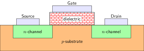
Наиболее часто используемый транзистор — это metal–oxide–semiconductor field-effect transistor (MOSFET, полевой транзистор со структурой металл-оксид-полупроводник), обычно называемый MOS-транзистором. По принципу работы MOS-транзисторы делятся на два типа: nMOS (MOS n-типа, где N означает Negative, «отрицательный») и pMOS (MOS p-типа, где P означает Positive, «положительный»). У обоих типов по три вывода: затвор, исток и сток. Их виды сбоку показаны на рисунке ниже.
 |  |
|---|
Транзисторы обычно используются как компоненты схем и подключаются в схему подобно переключателям. В повседневной жизни переключатели, как правило, управляются вручную, например выключатель света. Когда переключатель включён, цепи, подключённые к его двум выводам, соединяются между собой. В отличие от переключателей с ручным управлением, транзистор — это особый переключатель, управляемый напряжением в схеме. Управляя напряжением на затворе MOS-транзистора, мы можем определять, соединены ли его исток и сток.
Рассмотрим в качестве примера nMOS-транзистор: его поведение можно описать на основе электрических характеристик следующим образом:
- Когда разность напряжений между затвором и истоком, , достаточно велика, исток и сток проводят ток, что эквивалентно замыканию переключателя.
- Когда разность напряжений между затвором и истоком, , мала, исток и сток отсечены, что эквивалентно размыканию переключателя.
pMOS-транзистор ведёт себя аналогично nMOS-транзистору. Он проводит ток, когда достаточно велико, и отсечён, когда мало.
Как транзистор работает как переключатель, управляемый напряжением?
Чтобы разобраться в этом вопросе, нужны некоторые знания школьной физики и химии. Однако эта тема выходит за рамки проектирования процессоров и не является чем-то обязательным для освоения в процессе обучения по программе «One Student One Chip». Если вам интересно, мы можем дать краткое объяснение.
Кремний — основной материал, используемый для производства полупроводников. Два атома кремния, у каждого из которых по четыре валентных электрона, легко образуют устойчивые ковалентные связи. Поэтому чистый кремний не проводит электричество.
Рассмотрим в качестве примера изготовление nMOS: в кремний добавляют небольшое количество примеси элемента III группы, например бора, чтобы получить подложку p-типа, обозначенную на рисунке выше как p-substrate. Атом примеси в подложке p-типа образует устойчивые ковалентные связи с четырьмя соседними атомами кремния, но ему не хватает одного электрона. Поэтому он легко может притянуть электрон из другой ковалентной связи. Как только электрон покидает своё исходное место, это место может снова притянуть другой электрон и образовать ковалентную связь. По мере повторения этого процесса подложка p-типа ведёт себя так, будто содержит свободно перемещающиеся положительные заряды.
После формирования подложки p-типа над ней создаются две области n-типа, обозначенные на рисунке выше как n-channel, для чего в кремний добавляют небольшое количество примеси элемента V группы, например фосфора. Атом примеси в области n-типа образует устойчивые ковалентные связи с четырьмя соседними атомами кремния и имеет один лишний электрон. Этот электрон может свободно перемещаться в пределах области n-типа.
Чтобы подключить транзистор к источнику питания, от двух областей n-типа выводят два металлических электрода, которые используются как исток и сток. Затем поверх подложки наносится слой диоксида кремния в качестве изолирующего диэлектрического слоя, обозначенного на рисунке выше как dielectric. Ещё один металлический электрод размещается поверх диэлектрического слоя и служит затвором.
Во время работы исток и сток подключены к источнику питания и схеме. По умолчанию свободные электроны в области истока n-типа не могут пересечь подложку p-типа, чтобы достичь области стока n-типа. Поэтому исток и сток не проводят ток, и nMOS-транзистор находится в состоянии отсечки.
Когда на затвор подаётся достаточно высокое напряжение, под диэлектрическим слоем формируется электрическое поле. Под действием этого поля свободно перемещающиеся электроны в подложке p-типа движутся к диэлектрическому слою. Поскольку электроны не могут пройти через диэлектрик, они накапливаются под ним и образуют проводящий канал. Этот канал соединяет исток и сток, переводя nMOS-транзистор в состояние проводимости.
pMOS-транзистор работает по принципу, схожему с nMOS-транзистором, хотя они не полностью одинаковы. Заинтересованные студенты могут самостоятельно найти дополнительную информацию.
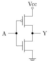
Поскольку у nMOS- и pMOS-транзисторов взаимодополняющие характеристики, в цифровых схемах их обычно используют вместе. Это называется технологией комплементарных структур металл-оксид-полупроводник (complementary metal–oxide–semiconductor, CMOS). Ниже показана одна из простейших CMOS-схем:
 |  |  |
|---|
Эта CMOS-схема работает следующим образом:
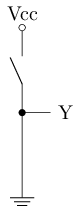
- Когда в точке A высокое напряжение, нижний nMOS-транзистор проводит, а верхний pMOS-транзистор отсечён. Это эквивалентно подключению точки Y к земле, как показано на среднем рисунке, поэтому напряжение в точке Y низкое.
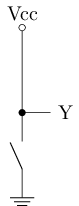
- Когда в точке A низкое напряжение, нижний nMOS-транзистор отсечён, а верхний pMOS-транзистор проводит. Это эквивалентно подключению точки Y к источнику питания, как показано на правом рисунке, поэтому напряжение в точке Y высокое.
Как видно, CMOS-схема преобразует переключающие свойства nMOS- и pMOS-транзисторов в высокое и низкое выходное напряжение. Определив физически высокое напряжение, например 5 В, как логическую 1 (высокий уровень), а низкое напряжение, например 0 В, как логический 0 (низкий уровень), мы получаем два базовых состояния сигнала, используемых в цифровых схемах.
Построение логических элементов из транзисторов
Одного лишь представления 0 и 1 недостаточно. Нам также нужно использовать CMOS-схемы, чтобы выполнять над 0 и 1 различные осмысленные преобразования. Этот процесс называется выполнением операций над цифровыми сигналами.
Элемент NOT (инвертор)
Рассмотрим CMOS-схему выше. Когда на входе в точке A 1, на выходе в точке Y получается 0; когда на входе в точке A 0, на выходе в точке Y получается 1. Это в точности логическая операция NOT. Такая схема называется элементом NOT, или инвертором.
 |
|---|
Элемент NAND
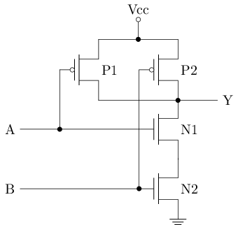
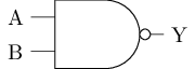
Теперь рассмотрим другую схему элемента ниже.
 |  |
|---|
Понять его функцию, просто взглянув на структуру схемы, непросто, поэтому нужно проанализировать его поведение. А именно: поскольку P1 и P2 соединены параллельно, Y равно 1, если проводит хотя бы один из них. Кроме того, поскольку N1 и N2 соединены последовательно, Y равно 0 только тогда, когда проводят оба. Поэтому поведение схемы можно свести в следующую таблицу:
| A | B | P1 | P2 | N1 | N2 | Y |
|---|---|---|---|---|---|---|
| 0 | 0 | проводимость | проводимость | отсечка | отсечка | 1 |
| 0 | 1 | проводимость | отсечка | отсечка | проводимость | 1 |
| 1 | 0 | отсечка | проводимость | проводимость | отсечка | 1 |
| 1 | 1 | отсечка | отсечка | проводимость | проводимость | 0 |
Согласно таблице выше, схема выдаёт 0, когда оба входа равны 1; в остальных случаях она выдаёт 1. Это в точности логическая операция NAND, поэтому эта схема — элемент NAND.
Элемент AND
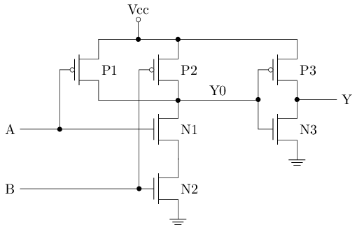
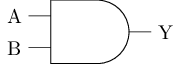
Если подключить выход элемента NAND ко входу элемента NOT, получится элемент AND. По сравнению с условным обозначением элемента NAND, у обозначения элемента AND на выходе нет кружка инверсии. В условных обозначениях логических элементов этот кружок указывает на инверсию.
 |  |
|---|
Проанализируйте схему элемента
Попробуйте проанализировать поведение и функцию следующей схемы элемента.
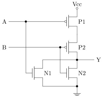 |
|---|
Транзисторная структура элемента OR
Ниже показано условное обозначение элемента OR. Попробуйте нарисовать его схему на уровне транзисторов.
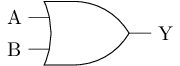 |
|---|
Трёхвходовый элемент NAND
Все рассмотренные выше схемы элементов имеют два входа. Однако иногда нам нужно выполнять операции над несколькими входными сигналами. Один из примеров — трёхвходовый элемент NAND. Его поведение можно выразить булевым выражением Y = ~(A & B & C), где & обозначает операцию AND. Опираясь на это выражение, можно построить трёхвходовый элемент NAND из двухвходового элемента AND и двухвходового элемента NAND, как показано на левом рисунке. Также трёхвходовый элемент NAND можно построить напрямую из транзисторов, как показано на правом рисунке.
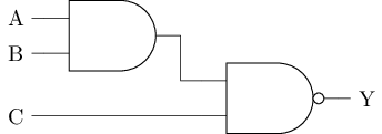 | 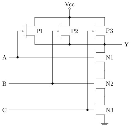 |
|---|
Сравните количество транзисторов, необходимое для двух реализаций
Нетрудно проанализировать, что приведённая выше транзисторная структура также реализует функцию трёхвходового элемента NAND. Попробуйте сравнить количество транзисторов, необходимое для двух реализаций.
Подсказка: для конструкций, построенных из схем элементов, количество транзисторов можно считать суммой количества транзисторов, использованных во всех схемах элементов конструкции.
Полностью заказные схемы: проектирование схем на уровне транзисторов
Схема, спроектированная непосредственно на уровне транзисторов, называется полностью заказной схемой (full-custom circuit). На примере трёхвходового элемента NAND видно, что полностью заказная схема требует меньше транзисторов и, соответственно, занимает меньшую площадь. В реальном производстве полностью заказные схемы также позволяют достичь более высокой тактовой частоты и меньшего энергопотребления.
Однако полностью заказные схемы сложно проектировать, и это требует длительного цикла разработки. Современные процессорные чипы часто содержат сотни миллионов транзисторов, поэтому разрабатывать весь чип методом полностью заказного проектирования непрактично. Для сверхбольших интегральных схем чаще применяются методы полузаказного проектирования.
Полузаказное проектирование схем можно дополнительно разделить на проектирование на основе стандартных ячеек и проектирование на основе вентильных матриц. При проектировании на основе стандартных ячеек часто используемые логические элементы, такие как элементы AND, OR и триггеры, сначала проектируются методом полностью заказного проектирования. Такие логические элементы называются стандартными ячейками, а из них затем строятся крупномасштабные схемы. Возвращаясь к примеру трёхвходового элемента NAND выше: если рассматривать двухвходовый элемент AND и двухвходовый элемент NAND как стандартные ячейки, то построение из них трёхвходового элемента NAND можно считать полузаказным проектированием. Распространённый пример проектирования на основе вентильных матриц — FPGA. Однако в дальнейших разделах мы не будем использовать FPGA. Заинтересованные студенты могут самостоятельно найти дополнительную информацию.
В современном проектировании процессоров в большинстве случаев используется полузаказное проектирование на основе стандартных ячеек. Полностью заказное проектирование применяется лишь для отдельных критически важных модулей, когда требуется предельная производительность, например когда коммерческие продукты конкурируют за долю рынка за счёт более высокой производительности.
Элемент XOR
Элемент XOR выполняет операцию исключающего ИЛИ (XOR). Его условное обозначение показано на рисунке ниже.
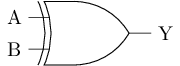 |
|---|
Исключающее ИЛИ — это особая операция, часто используемая при обработке логических данных. Её таблица истинности показана ниже:
| A | B | Y |
|---|---|---|
| 0 | 0 | 0 |
| 0 | 1 | 1 |
| 1 | 0 | 1 |
| 1 | 1 | 0 |
Операцию XOR можно понимать двумя способами:
- Слово «исключающее» указывает на «различие». Поэтому результат равен
1, когда входы A и B различаются; в противном случае результат равен0. - Операция OR даёт
1, если хотя бы один из двух входов равен1. В отличие от OR, XOR исключает случай, когда оба входа равны1. Поэтому она называется «исключающее ИЛИ» (exclusive OR), где «исключающее» соответствует слову exclusive. В противоположность этому операцию OR также называют «включающее ИЛИ» (inclusive OR), указывая на то, что случай, когда оба входа равны1, включён.
Из таблицы истинности можно вывести соответствующее булево выражение следующим образом:
- Постройте терм произведения для каждой комбинации входов. Для каждой строки таблицы истинности рассмотрите каждый входной сигнал. Если вход равен
1, используйте сам входной сигнал; если вход равен0, используйте его инверсию. Примените к этим сигналам операцию AND, чтобы получить описание этого терма произведения. Например, строка, в которойA = 1иB = 0, описывается какA & ~B. - Объедините термы произведения, для которых выход равен
1, с помощью операции OR, чтобы получить итоговое булево выражение. В таблице истинности XOR есть два случая, когда выход равен1:A = 1, B = 0, описываемый какA & ~B; иA = 0, B = 1, описываемый как~A & B. Применив операцию OR к этим двум описаниям, получаем булево выражение для XOR:Y = A ^ B = (A & ~B) | (~A & B).
Описанные выше шаги позволяют преобразовать таблицу истинности в булево выражение, состоящее из операций AND и OR. На основе этого булева выражения можно легко построить соответствующую схему, используя элементы AND и OR.
Упрощение с помощью карт Карно
Возможно, вы уже слышали об этом методе в каких-нибудь учебниках по цифровым схемам. Если нет — это, пожалуй, даже хорошо. Вам может понадобиться выучить его для экзамена, но в практическом проекте вроде «One Student One Chip» вы вряд ли будете его использовать.
Дело в том, что этот метод очень плохо масштабируется. В реальных проектах вам может понадобиться иметь дело с пятью и более переменными, а то и с десятками, и в таких случаях карты Карно крайне неэффективны для упрощения подобных выражений. На практике современные инструменты обычно упрощают булевы выражения с помощью таких алгоритмов, как алгоритм Куайна — Мак-Класки (QMC) или алгоритм Espresso. Поэтому вам редко придётся упрощать булевы выражения вручную. Описанного выше метода достаточно, чтобы вывести корректное булево выражение, а упрощением займутся современные инструменты. Заинтересованные студенты могут самостоятельно найти дополнительную информацию об этих алгоритмах.
Постройте элемент XOR из других логических элементов
В Logisim попробуйте построить элемент XOR, используя упомянутые выше логические элементы. После завершения схемы проверьте свою реализацию с помощью моделирования.
Когда ваша реализация заработает правильно, посчитайте, сколько транзисторов она использует.
Найдите более удачную реализацию
Не рассматривая полностью заказную схему, попробуйте найти реализацию элемента XOR, использующую наименьшее количество транзисторов, и проверьте свою конструкцию в Logisim.
Подсказка: одна из реализаций требует всего 14 транзисторов, поэтому оптимальная реализация должна использовать не более 14 транзисторов.
Полностью заказная схема для элемента XOR
На рисунке ниже показана одна из полностью заказных реализаций элемента XOR. Попробуйте проанализировать её поведение.
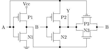 |
|---|
Спроектируйте элемент XNOR
Ещё одна операция — исключающее ИЛИ-НЕ (XNOR). Когда входы A и B совпадают, результат равен 1; в противном случае результат равен 0. Операцию XNOR можно рассматривать как инверсию операции XOR.
В Logisim попробуйте построить элемент XNOR, используя рассмотренные выше логические элементы. После завершения схемы проверьте свою реализацию с помощью моделирования.
Полностью заказная схема для элемента XNOR
Попробуйте построить элемент XNOR, используя как можно меньше транзисторов.
Подсказка: одна из реализаций требует всего 6 транзисторов, поэтому оптимальная реализация должна использовать не более 6 транзисторов.
Машинное представление целых чисел
Мы уже знаем, что CMOS-схемы могут представлять и обрабатывать 0 и 1. Однако в физическом мире, в котором мы живём, далеко не всё сводится к 0 и 1. Поэтому нам нужно рассмотреть, как различные виды информации из физического мира можно представить с помощью 0 и 1. Этот процесс представления называется кодированием. Поскольку в физическом мире существует множество видов информации, сначала мы рассмотрим, как представлять натуральные числа.
Двоичная система счисления
Базовое представление о числах у нас сложилось ещё с начальной школы, а то и с детского сада. В повседневной жизни мы пользуемся десятичной системой счисления. Значение десятичного числа — то есть фактическую числовую величину, которую оно обозначает — можно получить с помощью разложения в виде взвешенной суммы. Например, десятичное число 734 можно разложить следующим образом:
В общем случае для -разрядного числа с основанием , записанного как , его значение можно получить с помощью следующего разложения в виде взвешенной суммы:
Здесь называется основанием, а называется весом разряда .
Если положить и ограничить каждое значениями 0 или 1, мы получим двоичную систему счисления. Поскольку в десятичной системе тоже встречаются цифры 0 и 1, на письме обычно добавляют префиксы или нижние индексы, чтобы указать, что число двоичное. В некоторых языках программирования для обозначения двоичного числа используется префикс 0b, например 0b00101110; в некоторых учебниках используется нижний индекс , например . В этих хендаутах мы в основном используем префикс 0b. Например, значение двоичного числа 0b00101110 равно
Чтобы преобразовать двоичное число в десятичное, используйте следующее разложение в виде взвешенной суммы:
Чтобы преобразовать десятичное число в двоичное, нужно определить каждый двоичный разряд в разложении в виде взвешенной суммы. Для этого перепишем приведённое выше разложение следующим образом:
Из этой перезаписи видно, что если десятичное число последовательно делить на 2, то получаемые по порядку остатки соответствуют . Этот процесс вычисления можно представить с помощью метода последовательного деления на 2. Например, для десятичного числа 46:
2 | 46   -> 0          ^  младший бит
  +----                |
 2 | 23   -> 1         |
   +----               |
  2 | 11   -> 1        |
    +----              |
   2 | 5    -> 1       |
     +----             |
    2 | 2    -> 0      |
      +----            |
     2 | 1    -> 1     |  старший бит
       +----
         0 (частное равно нулю, конец)
Наконец, если расположить все остатки от старшего бита к младшему, получится 0b101110 — двоичное представление числа 46. Это согласуется с 0b00101110 из предыдущего примера, если отбросить ведущие 0.
Шестнадцатеричная система счисления
Хотя двоичные числа могут обрабатываться цифровыми схемами напрямую, человеку их трудно читать и запоминать. Например, сложно с первого взгляда определить количество разрядов в двоичном числе 0b1011111011101111. Кроме того, преобразование между двоичной и десятичной системами требует определённых вычислений, которые человеку, как правило, трудно выполнить быстро.
Чтобы решить эти проблемы, в областях, связанных с компьютерами, обычно используется шестнадцатеричная система счисления. В шестнадцатеричной системе каждый разряд может принимать 16 возможных значений. Помимо 0–9, буквы a, b, c, d, e и f (можно также использовать заглавные буквы) обозначают значения 10, 11, 12, 13, 14 и 15 соответственно. В некоторых языках программирования для обозначения шестнадцатеричного числа используется префикс 0x, например 0xbeef; в некоторых учебниках используется нижний индекс , например . В этих хендаутах мы в основном используем префикс 0x. Аналогично, преобразования между десятичной и шестнадцатеричной системами можно выполнять с помощью разложения в виде взвешенной суммы и последовательного деления. Например, разложение в виде взвешенной суммы для шестнадцатеричного числа 0xbeef выглядит так:
Хотя цифровые схемы не могут напрямую обрабатывать шестнадцатеричные числа, поскольку , один шестнадцатеричный разряд можно напрямую преобразовать в четыре двоичных разряда, и наоборот. Это значительно повышает эффективность преобразования между шестнадцатеричной и двоичной системами. Например, для двоичного числа 0b1011111011101111 можно разбить его разряды на группы по четыре, начиная справа налево, дополнив самую старшую группу ведущими 0, если в ней меньше четырёх разрядов, а затем записать для каждой группы соответствующую шестнадцатеричную цифру:
1011 1110 1110 1111
  |    |    |    |
  b    e    e    f
Таким образом, соответствующее шестнадцатеричное число — 0xbeef. По сравнению с двоичным представлением 0b1011111011101111, шестнадцатеричное представление 0xbeef гораздо компактнее и лаконичнее.
Восьмеричная система счисления
Восьмеричная система счисления также используется в некоторых вычислительных сценариях. Её принципы схожи с принципами шестнадцатеричной системы. Заинтересованные студенты могут самостоятельно вывести методы преобразования между восьмеричной и десятичной, а также между восьмеричной и двоичной системами.
Построение базовых комбинационных логических схем из логических элементов
С помощью логических элементов мы можем объединять несколько схем элементов, чтобы строить модули, часто используемые в цифровых схемах.
Дешифратор
Дешифратор — это схема, которая преобразует -битный вход не более чем в различных выходов. Распространённый тип дешифратора — дешифратор «1 из n», у которого входных битов и выходных битов. Он интерпретирует вход как двоичное число , устанавливает выход в 1, а все остальные выходы — в 0. Поскольку 1 установлена ровно в одном выходном бите, такой формат вывода также называют унитарным кодом (one-hot). Например, у дешифратора «2 в 4» два входных бита, , и четыре выходных бита, . Его таблица истинности и схема показаны ниже:
| 0 | 0 | 0 | 0 | 0 | 1 | |
| 0 | 1 | 0 | 0 | 1 | 0 | |
| 1 | 0 | 0 | 1 | 0 | 0 | |
| 1 | 1 | 1 | 0 | 0 | 0 |
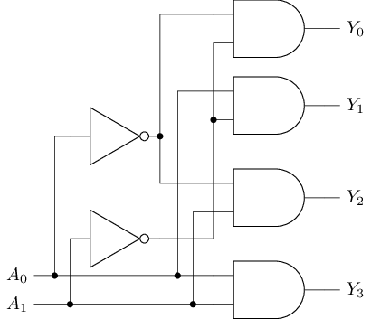 |
|---|
Постройте дешифратор «2 в 4»
В Logisim попробуйте построить дешифратор «2 в 4» из логических элементов. У него 2-битный вход и 4-битный выход. После завершения схемы проверьте свою реализацию с помощью моделирования.
В Logisim также есть готовые компоненты, такие как дешифраторы. Однако от вас всё равно требуется построить их из логических элементов, чтобы лучше понять фундаментальные принципы работы цифровых схем.
В компьютерах дешифраторы «1 из n» часто используются для реализации части процесса адресации. В этом случае входом дешифратора служит адрес, а его выходами — сигналы выбора. Сигнал выбора, соответствующий адресу, устанавливается в 1.
Настройка количества и полярности входов логического элемента
В Logisim можно настраивать количество и полярность входов логического элемента. Свойство полярности определяет, инвертируется ли сигнал перед тем, как попасть на вход логического элемента. Если инверсия включена, у соответствующего входного вывода появляется кружок, обозначающий инверсию. Подробные инструкции по настройке см. в разделе о логических элементах официальной документации.
Адреса и адресация
«Адрес» — это технический термин в вычислительной технике, но его также можно понять на примерах из повседневной жизни. Возможно, вы пользовались Excel для просмотра таблиц. Каждая строка таблицы хранит один элемент, и обычно несколько элементов хранятся подряд в порядке возрастания номера строки. Excel отображает номера строк слева, позволяя быстро определить, какую строку вы сейчас просматриваете. Чтобы найти элемент в строке 176, вам не нужно просматривать все строки начиная с первой. Вместо этого можно перетащить полосу прокрутки окна и быстро перейти к строке 176. Это возможно потому, что номера строк идут подряд, что позволяет эффективно пропускать предшествующие строки.
На самом деле, значительная часть данных в компьютере также хранится подряд, во многом подобно таблице. Например, память можно рассматривать как огромную таблицу, в которой каждая строка — это ячейка памяти, способная хранить один байт данных. Для модуля памяти объёмом 4 ГБ эта таблица содержит строк. Поскольку эти ячейки памяти расположены подряд, компьютеру не нужно просматривать их одну за другой начиная с первой, чтобы обратиться к конкретной ячейке. Вместо этого он может использовать «номер строки», чтобы сразу найти нужную ячейку памяти. Такой «номер строки» в вычислительной технике называется адресом, а процесс поиска ячейки памяти по её адресу называется адресацией.
Компьютер может быстро находить нужную ячейку памяти по адресу благодаря тому, что дешифратор «1 из n» способен быстро преобразовать адрес в группу сигналов выбора, которые затем используются для выбора нужных данных.
Подсхемы в Logisim
Дешифраторы будут часто использоваться в последующих проектах цифровых схем. Чтобы не проектировать одну и ту же схему заново каждый раз, в Logisim есть возможность подсхем: схему нужно спроектировать только один раз, а затем можно многократно создавать её экземпляры. Подробные инструкции см. в разделе Subcircuits официального руководства.
Освоив использование подсхем в Logisim, попробуйте оформить спроектированный вами дешифратор в виде подсхемы.
Расширение дешифратора
У дешифратора «3 в 8» 3-битный вход и 8-битный выход. Попробуйте создать несколько экземпляров дешифратора «2 в 4» — точное количество определите сами — и добавить небольшое число логических элементов, чтобы реализовать дешифратор «3 в 8». После завершения схемы проверьте свою реализацию с помощью моделирования.
В Logisim входные и выходные сигналы модуля обычно подключаются к компонентам ввода или вывода, состояние которых отображает текущие значения этих сигналов. Чтобы посмотреть текущее значение промежуточного сигнала, используйте компонент Probe из библиотеки компонентов. Его можно найти в категории Wiring библиотеки компонентов Logisim. RTFM для подробных инструкций по использованию.
Настройка разрядности компонентов
В Logisim можно настраивать разрядность данных компонента. Например, если разрядность элемента AND установлена в 4, каждый вывод может подключаться к 4-битному сигналу. Функционально это эквивалентно использованию четырёх 1-битных элементов AND, независимо обрабатывающих соответствующие биты четырёхбитных сигналов. Разрядность удобна для проектирования схем, выполняющих одну и ту же операцию сразу над несколькими битами. Подробные инструкции по настройке см. в разделе о логических элементах официальной документации.
Вам также может понадобиться извлечь несколько битов из группы сигналов или объединить несколько отдельных сигналов в одну группу для подключения. Для этого используйте компонент Splitter, который можно найти в категории Wiring библиотеки компонентов Logisim. RTFM для подробных инструкций по использованию.
Ещё один распространённый тип дешифратора — преобразователь кода, который по заданным правилам преобразует вход в одном кодировании в выход в другом кодировании. В отличие от дешифратора «1 из n», у преобразователя кода на выходе не обязательно должна быть не более одной 1.
Распространённое применение преобразователя кода — семисегментный дешифратор. Семисегментный индикатор — это компонент вывода, состоящий из семи светодиодов, расположенных в форме цифры 8, как показано на рисунке ниже. Буквы от a до g обозначают положения семи сегментов. Когда соответствующий управляющий сигнал активен, этот сегмент загорается. На рисунке также показана десятичная точка, обозначенная h, которая используется в приложениях, где нужно отображать десятичные дроби.
   a
  ---
f| g |b
  ---
e|   |c
  ---    .h
   d
Семисегментный дешифратор интерпретирует 4-битный вход как целое двоичное число и формирует группу управляющих сигналов, включающих или выключающих сегменты семисегментного индикатора, чтобы индикатор показывал цифру, соответствующую входу. Например:
вход     выход
         abcdefgh
0100     01100110
Приведённый выше пример показывает, как отобразить цифру 4 на семисегментном индикаторе. А именно, для отображения 4 нужно включить сегменты b, c, f и g, поэтому их управляющие сигналы должны быть активны. Здесь мы предполагаем, что сигналы активны при высоком уровне; на практике вам следует проверить полярность входов конкретного компонента семисегментного индикатора. Управляющие сигналы остальных сегментов должны быть неактивны. Если расположить выходы от a до h слева направо, выходные управляющие сигналы должны быть 01100110. Поскольку двоичное представление 4 — это 0b0100, семисегментный дешифратор должен выдавать 01100110, когда его вход равен 0100. Аналогично можно вывести шаблоны входа и выхода для цифр от 0 до 9.
Постройте семисегментный дешифратор
В Logisim попробуйте построить семисегментный дешифратор из логических элементов. У него 4-битный вход и 8-битный выход, подключённые соответственно к DIP switch и семисегментному индикатору. Дешифратор должен поддерживать отображение десятичных цифр: когда вход представляет цифру от 0 до 9, семисегментный индикатор должен показывать соответствующую цифру; при всех остальных значениях входа должна отображаться только десятичная точка. После завершения схемы проверьте свою реализацию с помощью моделирования.
Подсказка:
- Компонент семисегментного индикатора можно найти в библиотеке компонентов. После создания его экземпляра наведите курсор мыши на вывод, чтобы увидеть описание его функции.
- Сначала можно использовать дешифратор «1 из n», чтобы получить унитарный код, а затем с помощью слоя элементов OR определить, при каких значениях входа должен включаться каждый сегмент.
Постройте семисегментный дешифратор (2)
В Logisim попробуйте построить из логических элементов семисегментный дешифратор, поддерживающий шестнадцатеричные цифры. В дополнение к описанным выше десятичным цифрам, когда вход представляет значение от 10 до 15, семисегментный индикатор должен показывать A, b, C, d, E и F соответственно. После завершения схемы проверьте свою реализацию с помощью моделирования.
Шифратор
Шифратор выполняет функцию, обратную дешифратору «1 из n»: он преобразует унитарный код в соответствующее двоичное значение. А именно, у шифратора входных битов и выходных битов. Если вход представляет собой корректный унитарный код и бит равен 1, на выходе получается двоичное представление . Если вход не является корректным унитарным кодом, выход не определён.
Например, у шифратора «4 в 2» четыре входных бита, , и два выходных бита, . Его таблица истинности показана ниже. Когда вход не является корректным унитарным кодом, выход обозначается как x, указывая на то, что он не определён и может принимать любое значение.
| 0 | 0 | 0 | 1 | 0 | 0 | |
| 0 | 0 | 1 | 0 | 0 | 1 | |
| 0 | 1 | 0 | 0 | 1 | 0 | |
| 1 | 0 | 0 | 0 | 1 | 1 | |
| про | чие | усло | вия | X | X |
Что значит «выход не определён»
Некоторые операции или модули дают осмысленный результат только при выполнении определённых предусловий. Один из примеров — деление в математике. Вы наверняка слышали фразы вроде «на ноль делить нельзя». Однако «нельзя» — это выражение из естественного языка, а не из языка математики. Точнее говоря, ненулевой делитель — это предусловие для деления. Когда делитель равен 0, это предусловие больше не выполняется, поэтому корректный и осмысленный результат определить невозможно. Поэтому и говорят, что результат не определён.
Пример с шифратором аналогичен. Корректный унитарный вход — это предусловие для правильной работы шифратора. Когда вход не является унитарным, это предусловие не выполняется, поэтому корректный и осмысленный выход определить невозможно.
Отсюда следует своего рода контракт использования: если пользователи ожидают от шифратора корректных результатов, они должны обеспечить выполнение предусловия — подать корректный унитарный вход. И наоборот, если это предусловие не выполнено, пользователь нарушил контракт. В этом случае выход шифратора не определён, и ответственность за любые последствия, вызванные обработкой этого неопределённого выхода последующими схемами, лежит на пользователе.
На уровне цифровой схемы каждый выходной сигнал шифратора обязан быть либо 0, либо 1. Однако когда выход не определён, ни одно из этих значений не несёт практического смысла. Поэтому разработчик шифратора может присвоить выходным сигналам в этих неопределённых случаях любое из значений. Согласно описанному выше контракту использования, пользователи шифратора не должны допускать, чтобы последующие схемы обрабатывали эти неопределённые выходные сигналы.
Поэтому при проектировании шифратора нам не нужно рассматривать его выходы при остальных входных условиях. Нужно лишь обеспечить, чтобы он давал корректный выход, когда вход унитарный:
Постройте шифратор
В Logisim попробуйте построить шифратор «16 в 4» из логических элементов. У него 16-битный вход и 4-битный выход, подключённые соответственно к DIP switch и семисегментному дешифратору, так чтобы выход шифратора отображался на семисегментном индикаторе как шестнадцатеричная цифра. После завершения схемы проверьте свою реализацию с помощью моделирования.
В компьютерах шифраторы часто используются для формирования соответствующего адреса из сигналов выбора, представленных унитарным кодом. Функцию шифратора можно понимать и иначе: он определяет позицию 1 в унитарном коде.
Рассмотренный выше шифратор требует, чтобы пользователь гарантировал унитарность входа. Чтобы получать содержательную информацию даже тогда, когда вход не унитарный, нужен другой тип шифратора — приоритетный шифратор. У приоритетного шифратора входных битов и выходных битов. В отличие от рассмотренного выше шифратора, приоритетный шифратор допускает, что в 1 могут быть сразу несколько входных битов. В этом случае кодируется старшая по позиции 1. Поэтому, если вход не полностью нулевой, выход указывает позицию старшей 1; если вход полностью нулевой, выход не определён.
Например, у приоритетного шифратора «4 в 2» четыре входных бита, , и два выходных бита, . Его таблица истинности показана ниже.
| 0 | 0 | 0 | 1 | 0 | 0 | |
| 0 | 0 | 1 | X | 0 | 1 | |
| 0 | 1 | X | X | 1 | 0 | |
| 1 | X | X | X | 1 | 1 | |
| 0 | 0 | 0 | 0 | X | X |
Постройте приоритетный шифратор «4 в 2»
Опираясь на таблицу истинности выше, попробуйте вывести булево выражение для каждого выходного бита. Затем постройте приоритетный шифратор «4 в 2» из логических элементов в Logisim. После завершения схемы проверьте свою реализацию с помощью моделирования.
После завершения реализации сравните количество логических элементов, необходимых шифратору «4 в 2» и приоритетному шифратору «4 в 2».
Расширение приоритетного шифратора
У приоритетного шифратора «16 в 4» 16 входных битов и 4 выходных бита. Попробуйте создать несколько экземпляров приоритетного шифратора «4 в 2» и добавить небольшое число логических элементов, чтобы реализовать приоритетный шифратор «16 в 4». Затем подключите приоритетный шифратор «16 в 4» к DIP switch и семисегментному дешифратору так, чтобы его выход отображался на семисегментном индикаторе как шестнадцатеричная цифра. После завершения схемы проверьте свою реализацию с помощью моделирования.
Подсчёт старших и младших нулей и единиц
Компьютерам иногда нужно подсчитывать количество старших нулей в машинном слове — то есть количество идущих подряд 0 начиная со старшего бита его двоичного представления. Пусть разрядность данных — 16 бит. Для значения 16392, двоичное представление которого — 0b0100000000001000, количество старших нулей равно 1.
Аналогично можно определить количество младших нулей как количество идущих подряд 0 начиная с младшего бита машинного слова. Снова возьмём 16392 в качестве примера: количество младших нулей равно 3. Старшие единицы и младшие единицы определяются таким же образом.
Подумайте, как эти значения можно эффективно вычислить с помощью приоритетного шифратора.
Мультиплексор
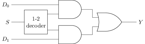
Мультиплексор выбирает один из нескольких входов данных в соответствии со своим управляющим входом выбора и передаёт выбранные данные на выход. Мультиплексор также называют MUX, или просто селектором. Простейший мультиплексор — это 1-битный мультиплексор «2 в 1», который выбирает один из двух 1-битных входов данных в соответствии с входом выбора. Его условное обозначение, структура схемы и таблица истинности показаны ниже.
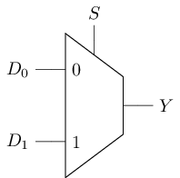 |  |
|---|
| 0 | ||
| 1 |
Как видно, мультиплексор содержит дешифратор «1 из n». Если рассматривать сигнал выбора мультиплексора как адрес, дешифратор формирует соответствующие сигналы выбора. Эти сигналы позволяют выбранному входу данных пройти через элемент AND, в то время как невыбранные входы данных после прохождения через свои элементы AND принудительно обнуляются. Наконец, элемент OR передаёт выбранные данные на выход.
Постройте 1-битный мультиплексор «2 в 1»
В Logisim попробуйте построить 1-битный мультиплексор «2 в 1» из логических элементов. После завершения схемы проверьте свою реализацию с помощью моделирования.
Мультиплексоры часто используются в компьютерах, потому что компьютеры по своей сути предназначены для обработки данных, а данные могут поступать из множества источников и обрабатываться множеством разных способов. Поэтому требуется большое количество мультиплексоров, чтобы выбирать между источниками данных и результатами обработки.
Постройте 3-битный мультиплексор «4 в 1»
Попробуйте нарисовать структуру схемы 3-битного мультиплексора «4 в 1», а затем постройте его из логических элементов в Logisim. После завершения схемы проверьте свою реализацию с помощью моделирования.
Подсказка:
- Если вам непонятно, что значит «3-битный мультиплексор «4 в 1»», внимательно перечитайте описание «1-битного мультиплексора «2 в 1»» выше.
- Для каждого бита входов данных сигналы выбора, сформированные дешифратором «1 из n», можно использовать, чтобы выбрать соответствующий вход.
Постройте семисегментный индикатор с переключаемой системой счисления
Используя пять DIP switch и один семисегментный индикатор, реализуйте следующую функцию: четыре DIP switch служат входом данных, а оставшийся DIP switch выбирает систему счисления. Когда сигнал выбора равен 0, семисегментный индикатор показывает вход в десятичной системе; когда сигнал выбора равен 1 — в шестнадцатеричной. Два режима отображения различаются, когда значение входа находится между 10 и 15.
Компаратор
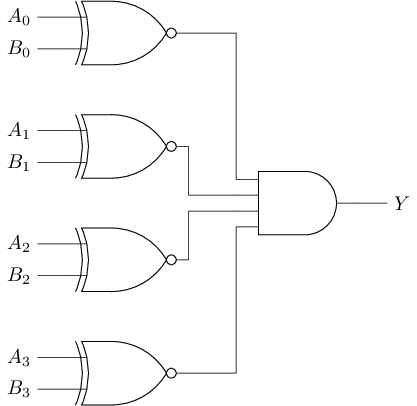
Компаратор проверяет, совпадают ли все соответствующие биты двух входов. Поскольку элементы XOR и XNOR умеют сравнивать два 1-битных значения, многобитный компаратор можно построить из элементов XOR или XNOR. На рисунке ниже показана структура схемы 4-битного компаратора.
 |
|---|
Постройте компаратор
В Logisim попробуйте построить 4-битный компаратор из логических элементов. Затем используйте две группы DIP switch, чтобы определять, равны ли две группы данных. Если они равны, включайте LED. После завершения схемы проверьте свою реализацию с помощью моделирования.
Сумматор
Сложение — основа арифметических операций, поэтому нам нужно рассмотреть, как реализовать его с помощью логических элементов. Сначала рассмотрим 1-битный сумматор. Входами операции сложения служат два слагаемых, а выходом — сумма . Поскольку сложение может порождать перенос, для сохранения этой информации также нужен выходной перенос . Опираясь на правила сложения, легко вывести таблицу истинности 1-битного сумматора.
A | B | S | C | |
|---|---|---|---|---|
| 0 | 0 | 0 | 0 | |
| 0 | 1 | 1 | 0 | |
| 1 | 0 | 1 | 0 | |
| 1 | 1 | 0 | 1 |
А именно, сумма равна 1 тогда и только тогда, когда два слагаемых различны, а перенос равен 1 тогда и только тогда, когда оба слагаемых равны 1. Из таблицы истинности получаем булевы выражения для и : S = A ^ B, C = A & B.
Для многобитного сумматора перенос, сформированный младшим битом, должен участвовать в сложении на следующем, более старшем бите. Поэтому нам нужно спроектировать новый сумматор, принимающий перенос от младшего бита в качестве входа. А именно, у этого сумматора три входа: A, B и Cin, где Cin обозначает входной перенос от младшего бита; и два выхода: S и Cout, где Cout обозначает выходной перенос, сформированный сложением. Чтобы отличать его от описанного выше сумматора, сумматор со входным переносом называется полным сумматором (full adder, FA), а описанный выше сумматор без входного переноса называется полусумматором (half adder, HA).
Постройте 1-битный полный сумматор
Попробуйте вывести таблицу истинности 1-битного полного сумматора, а затем постройте 1-битный полный сумматор из логических элементов в Logisim. После завершения схемы проверьте свою реализацию с помощью моделирования.
Постройте 1-битный полный сумматор (2)
Попробуйте создать несколько экземпляров полусумматора и добавить небольшое число логических элементов, чтобы реализовать 1-битный полный сумматор. После завершения схемы проверьте свою реализацию с помощью моделирования.
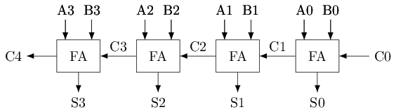
С помощью полного сумматора можно построить многобитный сумматор. Например, на рисунке ниже показана структура схемы 4-битного сумматора. Как видно, многобитный сумматор работает во многом подобно сложению многоразрядных чисел, изученному в начальной школе: вычисление выполняется разряд за разрядом, от младшего бита к старшему. Разница в том, что в школьной арифметике используется десятичное сложение, а здесь схема выполняет двоичное сложение. Такой тип многобитного сумматора называется сумматором с последовательным переносом (ripple-carry adder, RCA), потому что перенос, формируемый в ходе вычисления, распространяется от младших битов к старшим подобно волне (ripple).
 |
|---|
Постройте 4-битный сумматор
В Logisim попробуйте построить 4-битный сумматор из логических элементов. Используйте семисегментные индикаторы, чтобы отображать оба входа сумматора и результат в шестнадцатеричном виде, а также используйте LED, чтобы показывать, порождает ли сложение выходной перенос. После завершения схемы проверьте свою реализацию с помощью моделирования.
Представление целых чисел на уровне машины
Вспомним пример двоичного представления, рассмотренный выше:
В этом представлении каждый двоичный разряд вносит вклад в величину значения. Такое представление называется беззнаковым двоичным целым числом, или просто беззнаковым числом. Для -битного беззнакового числа минимальное значение равно 0, а максимальное — . Реализованный вами выше сумматор — это, по сути, сумматор для беззнаковых чисел.
Как же тогда компьютеру представлять отрицательные целые числа? В математике отрицательное число записывают, ставя знак минус - перед его абсолютным значением, например -5. Поскольку компьютеры могут обрабатывать только двоичные данные, нужно рассмотреть, как кодировать в двоичном виде целые числа, включая отрицательные. Простой подход — использовать один двоичный бит для кодирования знака числа, а оставшиеся биты — для кодирования его абсолютного значения. Такое представление называется знаковым двоичным целым числом, или просто знаковым числом.
Прямой код
Прямой код — это интуитивно понятная схема кодирования. Старший бит — это знаковый разряд: 0 означает положительное число, а 1 — отрицательное. Остальные биты представляют абсолютное значение соответствующей величины. Например:
0b00000111 = 7
0b10000111 = -7
0b00100010 = 34
0b10100010 = -34
Рассмотрим выполнение сложения в прямом коде с помощью 8-битного RCA:
  0b00000111 (7)      0b10000111 (-7)      0b10000111 (-7)      0b00000111 (7)
 +0b00100010 (34)    +0b10100010 (-34)    +0b00100010 (34)     +0b10000111 (-7)
  ------------        ------------          ------------          ------------
  0b00101001 (41)     0b00101001 (41)       0b10101001 (-41)      0b10001110 (-14)
Исходя из приведённых выше наблюдений, можно сделать следующие выводы:
- Когда оба операнда положительны, результат, полученный при их сложении с помощью RCA и интерпретированный как число в прямом коде, совпадает с математической суммой значений, представленных двумя операндами. Поэтому в этом случае сложение в прямом коде можно выполнять непосредственно с помощью RCA.
- Когда оба операнда отрицательны, результат, полученный RCA, не совпадает с математическим результатом, причём расхождение возникает в знаковом разряде. Поэтому в этом случае схеме нужно особым образом обрабатывать знаковый разряд.
- Когда отрицателен только один операнд, результат, полученный RCA, не совпадает с математическим результатом. Могут быть неверны и знаковый разряд, и величина. Поэтому в этом случае RCA нельзя использовать напрямую для сложения в прямом коде.
На самом деле, при математическом вычислении третьего случая операнд с меньшей величиной нужно вычесть из операнда с большей величиной, а знак результата взять от операнда с большей величиной. Это означает, что сумматору в прямом коде также требуется вычитатель. Затем нужно выбрать правильный результат в зависимости от знаков и величин двух операндов.
Постройте 4-битный вычитатель
Следуя подходу, использованному при проектировании 4-битного сумматора, попробуйте построить 4-битный вычитатель из логических элементов в Logisim. Используйте семисегментные индикаторы, чтобы отображать оба входа вычитателя и результат в шестнадцатеричном виде, а также используйте LED, чтобы показывать, порождает ли вычитание заём. После завершения схемы проверьте свою реализацию с помощью моделирования.
Постройте 4-битный сумматор в прямом коде
Разобравшись, как работает сумматор в прямом коде, используйте такие компоненты, как сумматоры, вычитатели и мультиплексоры, чтобы построить в Logisim 4-битный сумматор в прямом коде. Чтобы отображать знаковый разряд, можно создать экземпляр дополнительного семисегментного индикатора: показывайте знак минус -, когда результат отрицателен, и оставляйте индикатор пустым в остальных случаях. После завершения схемы проверьте свою реализацию с помощью моделирования.
Обратный код
Обратный код — ещё одна схема кодирования, призванная решить проблемы, связанные с отрицательными числами при сложении в прямом коде. А именно, положительные числа и 0 представляются так же, как и в прямом коде. Отрицательное число представляется так: берётся прямой код соответствующего ему положительного числа, и все биты инвертируются. Например:
0b00000111 = 7
0b11111000 = -7
0b00100010 = 34
0b11011101 = -34
Рассмотрим выполнение сложения в обратном коде с помощью 8-битного RCA:
  0b00000111 (7)      0b11111000 (-7)      0b11111000 (-7)      0b00000111 (7)
 +0b00100010 (34)    +0b11011101 (-34)    +0b00100010 (34)     +0b11111000 (-7)
  ------------        ------------          ------------          ------------
  0b00101001 (41)     0b11010101 (-42)      0b00011010 (26)       0b11111111 (-0)
Исходя из приведённых выше наблюдений, можно сделать следующие выводы:
- Когда оба операнда положительны, результат, полученный RCA и интерпретированный как число в обратном коде, совпадает с математической суммой значений, представленных двумя операндами. Поэтому в этом случае сложение в обратном коде можно выполнять непосредственно с помощью RCA.
- Когда один из операндов отрицателен, результат, полученный RCA, не совпадает с математическим результатом. Хотя знаковый разряд верен, величина неверна.
- В частности, при сложении двух чисел, противоположных друг другу, результат согласно определению обратного кода всегда равен
0b11111111. Интерпретированное как число в обратном коде, его значение —-0. Если считать-0математическим значением0, результат RCA верен.
Однако при использовании -0 в качестве входа RCA снова получаются неверные результаты:
  0b00000111 (7)      0b11111000 (-7)
 +0b11111111 (-0)    +0b11111111 (-0)
  ------------        ------------
  0b00000110 (6)      0b11110111 (-8)
Приведённые выше примеры показывают, что RCA нельзя использовать напрямую для выполнения сложения в обратном коде. Один из способов реализовать сложение в обратном коде — сначала преобразовать каждый операнд из обратного кода в эквивалентный прямой код, вычислить результат с помощью сумматора в прямом коде, а затем преобразовать результат обратно в эквивалентный обратный код.
Постройте 4-битный сумматор в обратном коде
Следуя описанному выше подходу, попробуйте построить 4-битный сумматор в обратном коде в Logisim. После завершения схемы проверьте свою реализацию с помощью моделирования.
Постройте 4-битный сумматор в обратном коде (2)
На самом деле, чтобы получить корректный результат сложения в обратном коде, достаточно лишь немного скорректировать результат, полученный RCA. Рассмотрите несколько примеров сложения 3-битных чисел в обратном коде, выявите закономерность в расхождении результатов, а затем добавьте к RCA соответствующую схему, чтобы более простым способом построить 4-битный сумматор в обратном коде. После завершения схемы проверьте свою реализацию с помощью моделирования.
Дополнительный код
Дополнительный код — это кодирование целых чисел, наиболее часто используемое в современных компьютерах. Оно дополнительно устраняет расхождение «на единицу», возникающее при арифметике в обратном коде. А именно, положительные числа и 0 представляются так же, как и в прямом коде. Отрицательное число представляется так: все биты прямого кода соответствующего ему положительного числа инвертируются, а затем к результату прибавляется 1. Например:
0b00000111 = 7
0b11111001 = -7
0b00100010 = 34
0b11011110 = -34
Для -битного числа в дополнительном коде максимальное значение представляется как 0b011...11 и равно , а минимальное значение представляется как 0b100...00 и равно . Минимальное значение — особый случай в дополнительном коде, поскольку его нельзя получить, применив операцию «инвертировать все биты и прибавить 1» к соответствующему положительному значению. Например, в 8-битном дополнительном коде максимальное значение — 0b01111111 = 127; применение «инвертировать все биты и прибавить 1» даёт 0b10000001 = -127. Минимальное же значение — 0b10000000 = -128; применение «инвертировать все биты и прибавить 1» даёт 0b01111111 + 1 = 0b10000000 = -128, то есть само исходное значение. Это происходит потому, что 128 выходит за пределы диапазона, представимого 8-битным числом в дополнительном коде.
Пусть представление положительного целого числа в дополнительном коде — это , а представление противоположного ему числа в дополнительном коде — это . По определению дополнительного кода,
где обозначает поразрядную инверсию . Разложив двоичные представления обеих частей в виде взвешенных сумм, получаем
Кроме того, поскольку равно либо 0, либо 1, соответственно равно 1 или 0. Следовательно, .
Теперь рассмотрим числовое значение, представленное :
Таким образом, при разложении представления в дополнительном коде для получения его числового значения знаковому разряду можно присвоить вес . Например, раскладывая таким образом 0b11111001, получаем
что согласуется со значением, представленным этим кодом.
Рассмотрим выполнение сложения в дополнительном коде с помощью 8-битного RCA:
  0b00000111 (7)      0b11111001 (-7)      0b11111001 (-7)      0b00000111 (7)
 +0b00100010 (34)    +0b11011110 (-34)    +0b00100010 (34)     +0b11111001 (-7)
  ------------        ------------         ------------         ------------
  0b00101001 (41)     0b11010111 (-41)     0b00011011 (27)      0b00000000 (0)
Из этих наблюдений видно, что когда RCA выполняет сложение в дополнительном коде, результат остаётся математически корректным, даже если среди входов есть отрицательные числа. Это означает, что RCA можно использовать и для выполнения вычитания в дополнительном коде. Математически . Поскольку мы показали, что результат, полученный RCA, математически корректен независимо от значений и , получаем
A + (-B), вычисленное с помощью RCA = A + (-B) в математике = A - B в математике
Именно потому, что и сложение, и вычитание в дополнительном коде можно выполнять с помощью сумматора, современные компьютеры обычно используют дополнительный код для представления целых чисел.
Почему же выполнение сложения в дополнительном коде с помощью RCA даёт корректный результат? Рассмотрим в качестве примера 4-битные двоичные числа. Расположим все двоичные комбинации по часовой стрелке, сформировав модель циферблата:
              0000 (0)
      (-1) 1111  0001 (1)
   (-2) 1110   ^    0010 (2)
 (-3) 1101     |      0011 (3)
(-4) 1100      +       0100 (4)
 (-5) 1011            0101 (5)
   (-6) 1010        0110 (6)
      (-7) 1001  0111 (7)
              1000 (-8)
RCA выполняет сложение на уровне двоичных разрядов. Прибавление положительного целого числа эквивалентно перемещению указателя по часовой стрелке на позиций, а прибавление отрицательного числа эквивалентно перемещению его против часовой стрелки на позиций. Чтобы сложение в конкретном кодировании согласовывалось со своим математическим смыслом, числовые значения, представленные этим кодированием, тоже должны возрастать по часовой стрелке. Значения в скобках на рисунке выше иллюстрируют случай дополнительного кода. Как видно, пока не пересечена граница между 7 и -8, результат сложения в дополнительном коде, выполненного RCA, всегда согласуется с математическим результатом. Что происходит при пересечении этой границы, мы обсудим позже.
       Прямой код                             Обратный код
              0000 (0)                             0000 (0)
      (-7) 1111  0001 (1)                  (-0) 1111  0001 (1)
   (-6) 1110   ^    0010 (2)            (-1) 1110   ^    0010 (2)
 (-5) 1101     |      0011 (3)        (-2) 1101     |      0011 (3)
(-4) 1100      +       0100 (4)      (-3) 1100      +       0100 (4)
 (-3) 1011            0101 (5)        (-4) 1011            0101 (5)
   (-2) 1010        0110 (6)            (-5) 1010        0110 (6)
      (-1) 1001  0111 (7)                  (-6) 1001  0111 (7)
              1000 (-0)                            1000 (-7)
Прямой код и обратный код не обладают описанным выше свойством. А именно, у прямого кода есть две проблемы:
- Между
0b0000и0b1111есть разрыв. Хотя двоичные коды по обе стороны этой границы идут подряд, представляемые ими значения — нет. В результате вычисленный результат не согласуется со своим математическим смыслом. Например, вычисление0 + (-1)в прямом коде эквивалентно перемещению указателя против часовой стрелки на одну позицию от0, что даёт-7— это не согласуется с математическим результатом. - Кодирование отрицательных чисел устроено так, что представляемые ими значения убывают по часовой стрелке, нарушая требование о том, что значения должны возрастать по часовой стрелке. В результате вычисленный результат не согласуется со своим математическим смыслом. Например, вычисление
(-4) + 1в прямом коде эквивалентно перемещению указателя по часовой стрелке на одну позицию от-4, что даёт-5— это не согласуется с математическим результатом.
Инвертируя биты, обратный код делает так, что значения, представленные кодами отрицательных чисел, возрастают по часовой стрелке, тем самым устраняя вторую проблему прямого кода. Однако первая проблема остаётся. Например, вычисление 0 + (-1) в обратном коде эквивалентно перемещению указателя против часовой стрелки на одну позицию от 0, что даёт -0 — это не согласуется с математическим результатом.
Опираясь на обратный код, дополнительный код добавляет к кодированию ещё +1, поворачивая значения, представленные кодами отрицательных чисел, по часовой стрелке ещё на одну позицию и тем самым устраняя и первую проблему.
Почему они называются «обратный код» и «дополнительный код»?
На самом деле дополнение — это понятие из теории систем счисления. Чтобы вычесть число, можно вместо этого прибавить его дополнение.
В n-разрядной системе счисления с основанием b у числа есть два вида дополнений. Первое — это дополнение до основания, в данном случае называемое дополнением до b, и определяется как . Второе — это уменьшенное дополнение до основания, в данном случае называемое дополнением до , и определяется как . Оба дополнения можно использовать вместе с соответствующими методами вычислений для выполнения вычитания. В частности, при эти два дополнения — это дополнительный код и обратный код соответственно.
Подробнее см. на соответствующей странице Википедии.
Обнаружение переполнения
Вспомним анализ выше. Даже в дополнительном коде остаётся граница, на которой коды идут подряд, а представляемые ими значения — нет: граница между 0b0111...111 и 0b1000...000, представляющими соответственно максимальное и минимальное значения. Если сложение пересекает эту границу, вычисленный результат не будет согласовываться со своим математическим смыслом. Эта граница существует потому, что при любом фиксированном числе двоичных разрядов представимый диапазон конечен. Поэтому некоторые значения неизбежно оказываются вне этого диапазона, из-за чего представляемые значения не могут оставаться непрерывными бесконечно. Вычисление, результат которого выходит за пределы диапазона, представимого данным кодированием, называется переполнением. Очевидно, что при переполнении вычисленный результат не согласуется со своим математическим смыслом. Поэтому операции сложения обычно требуется определять, произошло ли переполнение результата.
С точки зрения модели циферблата, пересечение границы разрыва может происходить двумя способами:
- Перемещение указателя по часовой стрелке из области положительных чисел с пересечением границы в область отрицательных чисел
- Перемещение указателя против часовой стрелки из области отрицательных чисел с пересечением границы в область положительных чисел
С математической точки зрения эти два случая соответствуют:
- Сложению двух положительных чисел с получением отрицательного результата
- Сложению двух отрицательных чисел с получением положительного результата
С этой точки зрения, чтобы определить, произошло ли переполнение, достаточно рассмотреть сложение знаковых разрядов. Поскольку сложение знаковых разрядов тоже выполняется полным сумматором, можно рассмотреть таблицу истинности полного сумматора.
| переполнение | ||||||
|---|---|---|---|---|---|---|
| 0 | 0 | 0 | 0 | 0 | НЕТ | |
| 0 | 0 | 1 | 0 | 1 | ДА | |
| ... | ... | ... | ... | ... | ... |
Здесь показаны только первые две строки таблицы истинности. По двум входам и и входному переносу логика полного сумматора формирует выходной перенос и бит суммы . Чтобы определить, произошло ли переполнение, по знаковым разрядам двух операндов и результата достаточно рассмотреть только , и . Например, первый случай соответствует сложению двух положительных чисел с получением положительного результата, поэтому переполнения не происходит. Второй случай соответствует сложению двух положительных чисел с получением отрицательного результата, поэтому переполнение происходит.
Обнаружение переполнения при сложении в дополнительном коде
Дополните приведённую выше таблицу истинности и выведите булево выражение для условия переполнения. Затем добавьте в Logisim логику обнаружения переполнения к 4-битному сумматору. После завершения схемы проверьте свою реализацию с помощью моделирования.
Последовательностные логические схемы
У модулей, рассмотренных в предыдущем разделе, есть общее свойство: их выходы полностью определяются текущими входами. Однако описанных выше модулей недостаточно, чтобы реализовать любую схему. Например, электронным часам нужно выполнять операцию новые секунды = предыдущие секунды + 1, поэтому их текущий выход также зависит от их предыдущего значения.
Поэтому нам нужно реализовать новый тип схемы со следующими двумя свойствами: (1) она может считывать предыдущее состояние схемы, и (2) она может обновлять состояние схемы. Схема с такими свойствами называется последовательностной логической схемой. Она способна хранить состояние, и её выход определяется совместно текущим входом и предыдущим состоянием. В отличие от них, схемы, рассмотренные в предыдущем разделе, называются комбинационными логическими схемами — у них нет понятия предыдущего или текущего состояния.
Перекрёстно связанные инверторы
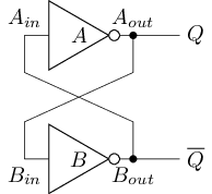
Для начала рассмотрим, как хранить и считывать состояние схемы. Простейшая схема, способная хранить состояние, — это пара перекрёстно связанных инверторов. Её структура показана ниже:
 |
|---|
Пусть суммарная задержка распространения сигнала от по проводу до , а затем через инвертор до , равна . Суммарная задержка распространения сигнала от по проводу до , а затем через инвертор до , также равна . Поведение схемы можно проанализировать для следующих четырёх случаев:
- Пусть изначально и , то есть и . Через время становится инверсией , то есть
1, а становится инверсией , то есть0. Таким образом, через время по-прежнему и , как и до времени $T`, поэтому состояние схемы не меняется. - Пусть изначально и , то есть и . Аналогичный анализ показывает, что через время по-прежнему и , как и до времени , поэтому состояние схемы не меняется.
- Пусть изначально и , то есть и . Через время становится инверсией , то есть
1, а становится инверсией , тоже1. Таким образом, через время получаем и $\overline{Q}=1`, поэтому состояние схемы меняется. - Пусть изначально и , то есть и . Аналогичный анализ показывает, что через время получаем и , поэтому состояние схемы меняется.
Из анализа выше следует, что при или схема остаётся в устойчивом состоянии. Мы считаем, что в этих случаях схема способна надёжно хранить 1 бит информации: когда и , схема хранит 0; когда и , схема хранит 1. Хранимое состояние можно считать с выхода .
Однако при или схема постоянно колеблется между этими двумя состояниями. Выход переключается между 0 и 1 и не может представлять устойчивую информацию. Такое состояние называется метастабильным. Оно может исказить другую информацию в схеме и привести к непредсказуемому поведению выхода схемы, поэтому его нужно избегать при проектировании схем.
В следующей таблице сведено поведение перекрёстно связанных инверторов:
| newQ | действие | ||||
|---|---|---|---|---|---|
| 0 | 0 | 1 | 1 | метастабильность | |
| 0 | 1 | 0 | 1 | запись 0 | |
| 1 | 0 | 1 | 0 | запись 1 | |
| 1 | 1 | 0 | 0 | метастабильность |
Однако даже когда перекрёстно связанные инверторы находятся в устойчивом состоянии, мы не можем обновить это состояние. Поскольку у схемы нет внешних входов, у нас нет способа управлять ею, что затрудняет её практическое использование. Чтобы решить эту проблему, нам нужен более практичный элемент хранения.
Перекрёстно связанные инверторы нельзя смоделировать в Logisim
Поскольку у перекрёстно связанных инверторов нет входов, Logisim не может определить их начальное состояние и поэтому не может корректно их смоделировать. Вам достаточно понимать, как работают перекрёстно связанные инверторы; выполнять какие-либо связанные с ними эксперименты не требуется.
SR-защёлка
SR-защёлка заменяет инверторы в паре перекрёстно связанных инверторов на элементы NOR, тем самым добавляя внешние управляющие входы. Здесь S означает set («установка»), и соответствующий управляющий вход устанавливает защёлку в 1; R означает reset («сброс»), и соответствующий управляющий вход сбрасывает защёлку в 0. Условное обозначение и структура схемы SR-защёлки показаны ниже.
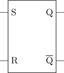 | 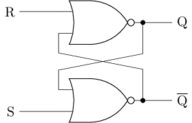 |
|---|
В зависимости от входов, поведение SR-защёлки можно проанализировать для четырёх случаев:
- Когда
S=1, R=0, верхний элемент NOR ведёт себя как инвертор, а выход нижнего элемента NOR принудительно устанавливается в0. В этом случае , поэтому значение, хранимое в SR-защёлке, обновляется до1. - Когда
S=0, R=1, выход верхнего элемента NOR принудительно устанавливается в0, а нижний элемент NOR ведёт себя как инвертор. В этом случае , поэтому значение, хранимое в SR-защёлке, обновляется до0. - Когда
S=0, R=0, оба элемента NOR ведут себя как инверторы. Поэтому SR-защёлка ведёт себя так же, как перекрёстно связанные инверторы, и сохраняет ранее хранимое значение. - Когда
S=1, R=1, выходы обоих элементов NOR принудительно устанавливаются в0, поэтому схема не может представлять корректную информацию. Более того, изменение входов сS=1, R=1наS=0, R=0эквивалентно переводу перекрёстно связанных инверторов в состояние . Как обсуждалось выше, это может привести SR-защёлку в метастабильное состояние, поэтому такого изменения нужно избегать.
В следующей таблице сведено поведение SR-защёлки:
S | R | Q | |
|---|---|---|---|
| 0 | 0 | сохранение | |
| 0 | 1 | 0 | |
| 1 | 0 | 1 | |
| 1 | 1 | недопустимо |
Постройте SR-защёлку
В Logisim попробуйте построить SR-защёлку из логических элементов. После завершения схемы проверьте свою реализацию с помощью моделирования.
При ручном управлении схемой невозможно одним щелчком изменить сразу два DIP switch с 11 на 00. Чтобы вызвать метастабильное состояние, можно добавить перед SR-защёлкой несколько элементов AND и использовать ещё один DIP switch, чтобы одновременно управлять одним входом каждого элемента AND. Это позволяет одним DIP switch одновременно обнулить оба входа SR-защёлки. Если вам удастся вызвать метастабильное состояние, Logisim выведет внизу окна сообщение Oscillation apparent. После этого моделирование не сможет продолжаться, и вам нужно будет сбросить его через меню Logisim.
SR-защёлка на элементах NAND
Рассмотренная выше SR-защёлка построена на элементах NOR. На самом деле элементы NOR можно заменить элементами NAND, получив защёлку, известную как -защёлка. Попробуйте вывести таблицу истинности -защёлки и проанализировать её поведение.
D-защёлка
Чтобы предотвратить метастабильность в самом источнике, можно добавить перед SR-защёлкой несколько логических элементов, ограничив её четыре комбинации входов тремя допустимыми комбинациями. В этом заключается основная идея D-защёлки. Её условное обозначение и структура схемы показаны ниже, где D — вход данных, а WE — разрешение записи.
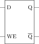 | 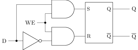 |
|---|
Проанализируйте поведение D-защёлки
Попробуйте вывести таблицу истинности по структуре схемы и проанализировать поведение D-защёлки.
Постройте D-защёлку
В Logisim попробуйте построить D-защёлку из логических элементов. После завершения схемы проверьте свою реализацию с помощью моделирования.
Постройте D-защёлку со сбросом
Попробуйте добавить к D-защёлке вход сброса и функцию сброса. Когда сигнал сброса активен, значение, хранимое в D-защёлке, должно становиться 0.
Реализуйте переключение бита с помощью D-защёлки
Создайте экземпляр D-защёлки с функцией сброса, инвертируйте её выход и подайте инвертированный сигнал обратно на её вход. Можно было бы ожидать, что выход D-защёлки будет переключаться между 0 и 1, но в моделировании должно появиться сообщение Oscillation apparent. Проанализируйте, почему так происходит.
Синхронные схемы
Сложная система содержит множество модулей, поэтому координация их работы — важный вопрос, который нужно учитывать. Например, пусть система содержит три модуля: модуль чтения данных, модуль сложения и модуль записи результата. Мы ожидаем, что следующие события произойдут в такой последовательности:
- Сначала работает модуль чтения данных.
- После того как данные прочитаны, модуль сложения начинает вычисление.
- После того как модуль сложения завершает вычисление результата, результат записывается в целевой элемент хранения.
Поэтому нам нужно установить отношение синхронизации, при котором событие A происходит после события B. Для этого требуется дополнительный механизм, и обычно применяются два подхода:
- Синхронная схема: синхронизация достигается с помощью глобального периодического тактового сигнала. Тактовый сигнал — это импульсный сигнал, как показано ниже, который чередует высокий и низкий уровни. Один интервал высокого уровня вместе с одним интервалом низкого уровня называется тактом. В синхронной схеме элемент хранения записывает данные только тогда, когда тактовый сигнал достигает переднего фронта (нарастающего фронта, перехода от низкого уровня к высокому) или заднего фронта (спадающего фронта, перехода от высокого уровня к низкому), а сохранённые данные можно надёжно считывать в последующих тактах. Благодаря этому свойству события, которые нужно синхронизировать, можно назначить на разные такты, позволяя тактовому сигналу управлять порядком их выполнения.
Пример тактового сигнала

             +--- передний фронт             +--- задний фронт
             V                               V
     +----+   +----+   +----+   +----+   +----+   +----+   +----+   +----+
     |    |   |    |   |    |   |    |   |    |   |    |   |    |   |    |
+----+    +---+    +---+    +---+    +---+    +---+    +---+    +---+    +
- Асинхронная схема: синхронизация достигается с помощью локальных сигналов связи между модулями.
По сравнению с асинхронными схемами синхронные схемы проще проектировать и анализировать. Хотя введение периодически переключающегося тактового сигнала приводит к более высокому энергопотреблению по сравнению с асинхронными схемами, синхронные схемы всё равно широко используются в промышленности. Наше дальнейшее изучение также будет основано на синхронных схемах.
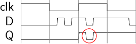
Однако D-защёлка не может удовлетворять требованиям к элементу хранения в синхронной схеме. Даже если подключить тактовый сигнал ко входу разрешения записи D-защёлки, приведённые выше требования всё равно не выполняются. Как показано на рисунке ниже, мы ожидаем, что данные будут записаны в элемент хранения при наступлении переднего фронта тактового сигнала и будут надёжно считываться из элемента хранения в последующих тактах. Однако область, обведённая красным на рисунке, нарушает это свойство.
 |
|---|
Это происходит потому, что защёлка — это элемент хранения, управляемый по уровню. Пока её вход меняется во время активного разрешения, защёлка немедленно обнаруживает это изменение и передаёт его на выход. В отличие от неё, нам нужен элемент хранения, управляемый по фронту, который передаёт свой вход на выход только при наступлении фронта сигнала.
D-триггер
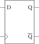
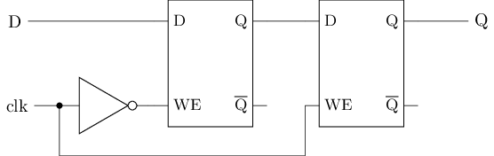
D-триггер — это элемент хранения, управляемый по фронту. Он строится из защёлок, но способен предотвращать распространение изменений входа, пока тактовый сигнал остаётся на постоянном уровне. Условное обозначение D-триггера показано ниже. Символ > в нижнем левом углу означает, что этот вывод нужно подключать к тактовому сигналу. D-триггеры можно реализовать несколькими способами. Здесь мы сначала рассмотрим D-триггер типа «ведущий-ведомый», структура которого показана ниже.
 |  |
|---|
D-триггер типа «ведущий-ведомый» состоит из двух D-защёлок. Защёлка слева называется ведущей защёлкой, а защёлка справа — ведомой защёлкой. Входы разрешения записи двух D-защёлок подключены соответственно к тактовому сигналу и его инверсии. Работу D-триггера типа «ведущий-ведомый» можно разделить на следующие фазы:
- Фаза подготовки данных: в этот момент тактовый сигнал
clkнаходится на низком уровне, поэтому вход разрешения записи ведущей защёлки активен, что позволяет сигналу данныхDпопадать в ведущую защёлку извне. Однако, поскольку вход разрешения записи ведомой защёлки неактивен, сигнал данных не может распространиться на ведомую защёлку, поэтому выходQвсего D-триггера остаётся неизменным. - Фаза выборки: когда наступает передний фронт
clk, вход разрешения записи ведущей защёлки становится неактивным, поэтому сигнал данныхDбольше не может попадать в ведущую защёлку извне. Последующие измененияDбольше не могут повлиять на ведущую защёлку, тем самым «запирая» внутри ведущей защёлки внешнее значениеD, присутствовавшее в момент переднего фронта. В то же время вход разрешения записи ведомой защёлки становится активным, что позволяет данным, «запертым» в ведущей защёлке, распространиться на ведомую защёлку и стать выходом всего D-триггера. - Фаза удержания: в этот момент тактовый сигнал
clkнаходится на высоком уровне, поэтому вход разрешения записи ведущей защёлки неактивен и, следовательно, не подвержен влиянию изменений сигнала данныхD. Хотя вход разрешения записи ведомой защёлки активен, ведущая защёлка остаётся неизменной, поэтому ведомая защёлка тоже остаётся неизменной, а выходQвсего D-триггера остаётся стабильным.
 |
|---|
В целом, когда наступает передний фронт тактового сигнала, данные записываются в D-триггер и затем могут надёжно считываться в последующих тактах, удовлетворяя требованиям к элементам хранения в синхронных схемах. Поэтому D-триггер — это базовый элемент хранения при проектировании синхронных схем.
Постройте D-триггер
Попробуйте построить D-триггер из логических элементов в Logisim. После завершения схемы подключите его тактовый вход к кнопке. Нажатие и отпускание кнопки дают соответственно высокий и низкий уровень, поэтому один щелчок по кнопке формирует импульс, который может служить тактовым сигналом. Попробуйте нажать и удерживать кнопку, чтобы понаблюдать за работой D-триггера типа «ведущий-ведомый».
Постройте D-триггер со сбросом
Попробуйте добавить к D-триггеру вход сброса и функцию сброса. Когда сигнал сброса активен, значение, хранимое в D-триггере, должно становиться 0.
Реализуйте переключение бита с помощью D-триггера
Создайте экземпляр D-триггера с функцией сброса, инвертируйте его выход и подайте инвертированный сигнал обратно на его вход. Мы ожидаем, что выход D-триггера будет переключаться между 0 и 1. Сравните результат с результатом для D-защёлки, описанной выше.
Постройте D-триггер, срабатывающий по заднему фронту
Описанный выше D-триггер типа «ведущий-ведомый» срабатывает по переднему фронту. Попробуйте построить D-триггер, срабатывающий по заднему фронту. После завершения схемы проверьте свою реализацию с помощью моделирования.
Другая реализация D-триггера
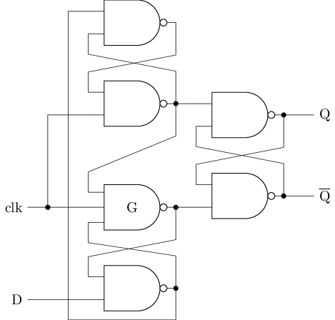
На рисунке ниже показана другая реализация D-триггера, известная как D-триггер типа hold-block. По сравнению с D-триггером типа «ведущий-ведомый» она накладывает меньше ограничений на свой вход. Заинтересованные студенты могут обратиться к соответствующим материалам, чтобы понять и проанализировать поведение D-триггера типа hold-block.
 |
|---|
Иногда мы не хотим, чтобы D-триггер обновлялся безусловно. Поэтому нам нужно добавить к D-триггеру вход разрешения, сформировав D-триггер с разрешением. Его условное обозначение показано ниже.
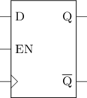 |
|---|
Постройте D-триггер с входом разрешения
Попробуйте построить в Logisim D-триггер с входом разрешения, используя D-триггеры и несколько дополнительных схем. После завершения схемы проверьте свою реализацию с помощью моделирования.
Регистр
Описанный выше D-триггер может хранить только 1 бит данных, но иногда нам нужно хранить и обрабатывать несколько битов как единое целое. Регистр — это элемент хранения, состоящий из нескольких D-триггеров. Его структура показана ниже. Эти D-триггеры используют общие тактовый сигнал и сигнал разрешения, что позволяет хранить несколько битов как единое целое.
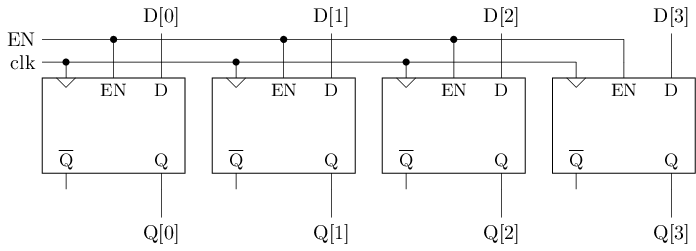 |
|---|
Постройте 4-битный регистр
В Logisim попробуйте построить 4-битный регистр из D-триггеров и добавить функцию сброса. После завершения схемы попробуйте записать в регистр 4-битные данные с DIP switch и подключить выход регистра к семисегментному индикатору.
Постройте 4-битный счётчик
Используя описанный выше 4-битный регистр и ранее построенный сумматор, реализуйте 4-битный счётчик. На каждом такте увеличивайте значение в регистре на 1. По достижении максимального значения счётчик должен переходить обратно к 0. В Logisim можно создать экземпляр константы с помощью компонента Constant из категории Wiring библиотеки компонентов. RTFM для подробных инструкций по использованию.
Спроектируйте схему суммирования последовательности
Попробуйте с помощью регистров и сумматоров вычислить результат 1+2+...+10. Можно рассмотреть реализацию 8-битных регистров и сумматоров, чтобы результат поместился.
Реализуйте цифровые часы
С помощью регистров и семисегментных индикаторов реализуйте цифровые часы, отображающие минуты и секунды.
Подсказка: компонент Clock может автоматически формировать тактовый сигнал, не требуя ручных щелчков, как в случае с кнопкой. Его можно найти в категории Wiring библиотеки компонентов Logisim. RTFM для подробных инструкций по использованию.