SoC Computer System
Bus Lecture Notes Updated
We added exercises on UART and CLINT to the bus section of our lecture notes on November 29, 2023. Completing these exercises will be beneficial for the upcoming SoC integration.
After implementing the bus, we can connect the NPC to the OSOC SoC environment, preparing for tape-out! SoC stands for System On Chip, which means that the SoC contains not just a processor, but also numerous peripheral devices, as well as the bus that connects the processor to these peripherals. Here, we consider memory as a type of peripheral device in a broad sense, since, for an SoC, memory and other narrower-defined devices are indistinguishable, which are all addressable spaces.
ysyxSoC
We provide an SoC environment that can run on Verilator, called ysyxSoC. We allow early access to ysyxSoC for two reasons: firstly, to make everyone learn about its details, and secondly, to test your NPC in the SoC environment as soon as possible. This helps shorten the time from completing the tape-out assessment to code submission. Of course, after integrating with ysyxSoC, you will still need to complete some optimization work to achieve the tape-out requirements for Phase B.
ysyxSoC Introduction
First, we present the peripheral devices included in ysyxSoC and their corresponding address spaces.
| Devices | Address Spaces |
|---|---|
| CLINT | 0x0200_0000~0x0200_ffff |
| SRAM | 0x0f00_0000~0x0fff_ffff |
| UART16550 | 0x1000_0000~0x1000_0fff |
| SPI master | 0x1000_1000~0x1000_1fff |
| GPIO | 0x1000_2000~0x1000_200f |
| PS2 | 0x1001_1000~0x1001_1007 |
| MROM | 0x2000_0000~0x2000_0fff |
| VGA | 0x2100_0000~0x211f_ffff |
| Flash | 0x3000_0000~0x3fff_ffff |
| ChipLink MMIO | 0x4000_0000~0x7fff_ffff |
| PSRAM | 0x8000_0000~0x9fff_ffff |
| SDRAM | 0xa000_0000~0xbfff_ffff |
| ChipLink MEM | 0xc000_0000~0xffff_ffff |
| Reverse | Others |
In addition to AXI, there are buses such as APB , wishbone and SPI in the figure. However, these buses are simpler than AXI, even simpler than AXI-Lite. You already know AXI-Lite, so it is not difficult to learn these bus protocols. You can read relevant manuals when necessary.
Some devices and address spaces may change in the future
In order to obtain a better display effect, the OSOC project team is redesigning the SoC. Some devices and address spaces may change in the future. The final device address space allocation is subject to the tape-out version. However, this does not affects your current learning, you can safely ignore this situation.
Get the source code of ysyxSoC
You need to clone the ysyxSoC project:
cd ysyx-workbench
git clone git@github.com:OSCPU/ysyxSoC.git
Next, you will use the devices provided by ysyxSoC for simulation in order to verify that the NPC can correctly access the devices in the SoC. We will introduce how to access it below.
It should be noted that there are still some differences between ysyxSoC and the SoC used in the final tape-out. Therefore, passing the test of ysyxSoC does not mean that it will eventually pass the test of the tape-out SoC simulation environment. But even so, some problems can be exposed in advance with the help of the ysyxSoC project, if there are still problems when connecting to the tape-out SoC in the future, you can focus on the impact of the differences between the two.
For everyone, there are two parts of the ysyxSoC project that deserve your attention. The first part is the bus of ysyxSoC, which we mainly use the diplomacy framework of the open source community rocket-chip project to implement it, the relevant code is in the ysyxSoC/soc/ directory. With diplomacy, we can easily connect the device with a bus interface to ysyxSoC. For example, we only need to change the following two lines of Chisel code to instantiate an AXI interface MROM device, specify its address space as 0x2000_0000~0x2000_0fff, and connect it to the downstream of AXI Xbar. If you use the traditional Verilog method, just port declaration will add nearly 100 lines of code, not counting the modification to AXI Xbar.
diff --git a/soc/SoC.scala b/soc/SoC.scala
index dd84776c..758fb8d1 100644
--- a/soc/SoC.scala
+++ b/soc/SoC.scala
@@ -35,9 +35,10 @@ class ysyxSoCASIC(implicit p: Parameters) extends LazyModule {
     AddressSet.misaligned(0x10001000, 0x1000) ++    // SPI controller
     AddressSet.misaligned(0x30000000, 0x10000000)   // XIP flash
   ))
+  val lmrom = LazyModule(new AXI4MROM(AddressSet.misaligned(0x20000000, 0x1000)))

   List(lspi.node, luart.node).map(_ := apbxbar)
-  List(chiplinkNode, apbxbar := AXI4ToAPB()).map(_ := xbar)
+  List(chiplinkNode, apbxbar := AXI4ToAPB(), lmrom.node).map(_ := xbar)
   xbar := cpu.masterNode

   override lazy val module = new Impl
The second part is the device of ysyxSoC. We have collected some open source projects of device controllers. The relevant codes are in ysyxSoC/perip/ directory. Some devices are implemented by directly instantiating the IP in the rocket-chip project. This part of the devices is not in ysyxSoC/perip/ directory. For details, please refer to the relevant code in ysyxSoC/soc/ .
Access ysyxSoC
Since the SoC contains multiple devices, the properties of these devices may be different, which will bring some new problems. For example, ysyxSoC/perip/uart16550/rtl/uart_defines.v has the following code:
// Register addresses
`define UART_REG_RB `UART_ADDR_WIDTH'd0  // receiver buffer
`define UART_REG_IE `UART_ADDR_WIDTH'd1  // Interrupt enable
`define UART_REG_II `UART_ADDR_WIDTH'd2  // Interrupt identification
`define UART_REG_LC `UART_ADDR_WIDTH'd3  // Line Control
The above code defines the addresses of some device registers in the UART. Since the UART is located at 0x1000_0000 , the addresses of the above four registers are 0x1000_0000 , 0x1000_0001 , 0x1000_0002 , 0x1000_0003 . Assuming that the UART is connected to Xbar through the AXI-Lite bus, consider reading contents of the receiver buffer through AXI-Lite. Obviously, araddr signal should be 0x1000_0000 , but if you want to read 4 bytes, will the contents of the next three device registers be read at the same time?
We did not consider the issue of "how much to read" before because when reading the memory, it does not change the state of the data stored in the memory. Therefore, no matter how many bytes the CPU expects to read, the bus can read 4 bytes or 8 bytes at a time, allowing the CPU to select the target data. This even helps some CPUs with caches to improve performance: reading data from memory once generally takes a long time. If the bandwidth of the bus can be fully utilized, it is possible to reduce the number of actual memory accesses by fetching more data during once access in the future.
However, for device access, the above premise is no longer true, accessing device registers may change the state of the devices! This means that for devices, reading 1 byte and reading 4 bytes may ultimately lead to different behaviors. If we do not access device registers according to their conventions, it may lead the devices to an unpredictable state. Therefore, we need to handle this issue carefully when accessing devices through the bus.
However, the AXI-Lite bus cannot solve the above problem. There is not enough signals in its AR channel to encode the read length information. The device can only think that the actually accessed data bit width is the same as the data bit width of the AXI-Lite bus. Therefore. , if a single read request on the AXI-Lite bus covers multiple device registers, it may cause an error in the device status. For this reason, not all devices are suitable for access through the AXI-Lite bus.
For example, the above UART cannot be accessed through the AXI-Lite bus with a data bit width of 32 bits, because the interval between device registers in the UART is only 1 byte, which means that reading one of the device registers through AXI-Lite will also affect the status of the corresponding device register, which is not what we expect. For another UART whose device register address space is as follows, it can be accessed through the AXI-Lite bus with a data bit width of 32 bits, because the interval between these registers is 4 bytes, just enough to read one of the registers without affecting the status of adjacent registers.
// Register addresses
`define UART_REG_RB `UART_ADDR_WIDTH'd0  // receiver buffer
`define UART_REG_IE `UART_ADDR_WIDTH'd4  // Interrupt enable
`define UART_REG_II `UART_ADDR_WIDTH'd8  // Interrupt identification
`define UART_REG_LC `UART_ADDR_WIDTH'd12 // Line Control
In order to solve the above problems of AXI-Lite, the complete AXI bus protocol uses the arsize / awsize signal to indicate the actual accessed data bit width, and also introduces the concept of "narrow transmission" to indicate that "the actual data bit width is less than the bus data bit width" situation. These two concepts of "data bit width" are not completely consistent. Specifically, the bus data bit width is statically determined during hardware design. It represents the maximum data bit width of a bus transmission and is also used to calculate the theoretical bandwidth of the bus. The actual data bit width (i.e., the value of the arsize / awsize signal) is dynamically determined by the bit width information in the software memory access instruction, which represents the actual data bit width of a bus transmission. For example, lb instruction only accesses 1 byte, while lw instruction accesses 4 bytes.
With arsize / awsize signal, the device will know the actual data bit width that the software needs to access, so that when the addresses of several device registers are closely arranged, it can only access one of the registers to avoid accidentally changing the state of the device.
Access ysyxSoC
Follow the steps below to access the NPC to ysyxSoC:
- According to
masterbus inysyxSoC/spec/cpu-interface.md, the previously implemented AXI4Lite protocol is extended to the complete AXI4 - Adjust the NPC top-level interface to be completely consistent with the interface naming specification in
ysyxSoC/spec/cpu-interface.md, including signal direction, naming and data bit width- For unused top-level output ports, they need to be assigned a constant value of
0 - For unused top-level input ports, just leave them floating.
- In order to be compatible with previous designs, we adopt a 64-bit data width interface. If your NPC is 32 bits, currently only the lower 32 bits of the data need to be used. We will discuss this issue again later.
- For unused top-level output ports, they need to be assigned a constant value of
- Add all
.vfiles in theysyxSoC/peripdirectory and its subdirectories to verilator's Verilog file list - Add the two directories
ysyxSoC/perip/uart16550/rtlandysyxSoC/perip/spi/rtlto the include search path of verilator- For details on how to join, please RTFM (
man verilatoror verilator’s official manual)- If you have never looked up the options of verilator, we recommend that you take this opportunity to carefully read
argument summaryin the manual. You may well discover some new treasures.
- If you have never looked up the options of verilator, we recommend that you take this opportunity to carefully read
- For details on how to join, please RTFM (
- Add
--timescale "1ns/1ns"and--no-timingto verilator compilation options - Set the
ysyxSoCFullmodule (defined inysyxSoC/generated/ysyxSoCFull.v) as the top-level module for verilator simulation- If you don't know how to join, RTFM
- Change the
ysyx_00000000module name inysyxSoC/generated/ysyxSoCFull.vto the module name of your processor- Note that this module should not contain the SRAM and UART of the AXI4-Lite interface as an exercise before, we will replace them with the memory and UART in ysyxSoC
- But this module should contain CLINT, which will be used as a module in the tape-out project, which ysyxSoC does not include.
- Add the following content to the simulated cpp file to solve the problem of
flash_readandmrom_readnot being found during linkingextern "C" void flash_read(uint32_t addr, uint32_t *data) { assert(0); } extern "C" void mrom_read(uint32_t addr, uint32_t *data) { assert(0); } - Add the statement
Verilated::commandArgs(argc, argv);inmainfunction of the simulation environment before the simulation starts to solve the problem of runtime errors reported by the plusargs function. - Compile the simulation executable file through verilator
- If you encounter a combined loopback error, please modify your RTL code yourself
- Try to start the simulation, you will observe that the code enters the main loop of the simulation, but the NPC has no valid output. We will solve this problem next
There are also some step instructions related to code inspection in ysyxSoC , but you will also need to improve the NPC in the future, so we will ask you to conduct code inspection before the assessment. If you are interested, you can also carry out code inspection at present, we will not require it.
Next, we will introduce the devices and how to let the program use them in ysyxSoC one by one. Some tasks will require you to implement or enhance some device modules on the RTL level. For most of these tasks, you can choose to use Chisel or Verilog to complete. In particular, if you choose to use Chisel, you will still need to read some Verilog code to help you complete the task.
Get the code of rocket-chip
If you prefer to use Chisel to complete subsequent tasks, or are interested in the details of the ysyxSoC bus part, you can obtain the rocket-chip code by obtaining the command as follows:
- Remove the comments of variable definitions at the beginning of
ysyxSoC/Makefile - Run the
make dev-initcommand in theysyxSoC/directory
In order to generate Verilog code, you also need to add the directory where firtool is located to PATH environment variable, and then run make verilog command in ysyxSoC/ directory. For details on adding firtool, please refer to the Chisel development environment we provide.
The simplest SoC
Recall that two of the elements of TRM are that a program can be executed and can be output. In the previous simulation process, these two points were realized through the simulation environment. The simulation environment puts the image file of the program into the memory, and when NPC fetches the first instruction, the program is already in the memory; for output, we use the DPI-C function pmem_read() to call the function of the simulation environment, and realize the output through putchar() function of the simulation environment. But in the real SoC , there is no simulation environment or runtime environment to provide the above functions after the board is powered on, so these basic functions need to be implemented through hardware.
Program storage
First, you need to consider where the program is placed. General memories are volatile memories, such as SRAM and DRAM, which do not store valid data when powered on. If the CPU directly reads instructions from the memory after powering on, what data is read out of the memory is undefined, so the behavior of the entire system is also undefined, making it impossible for the CPU to execute the expected program.
Therefore, it is necessary to use a non-volatile memory to store the original program so that its contents can be retained when the power is turned off, and the CPU can immediately retrieve instructions from it when the power is turned on. The simplest solution is ROM (Read-Only Memory). The content read from the same location in ROM is the same every time.
There are many ways to implement ROM. Generally speaking, information (also programs here) is stored in ROM in some way, and this storage method will not be affected by power outages, so it has non-volatile properties. If you consider the ease of use in ysyxSoC, the most suitable one is mask ROM (mask ROM), referred to as MROM. Its essence is to "hard-code" information in the gate circuit, so the access method is very direct for NPC.
However, due to some problems with MROM, we do not plan to use it during tape-out. However, MROM, as the first simple non-volatile memory in ysyxSoC to store programs, is very suitable for us to test the access of ysyxSoC. We have added an AXI4 interface MROM controller to ysyxSoC, and its address space is 0x2000_0000~0x2000_0fff.
Test MROM access
Modify the reset PC value of NPC so that it fetches the first instruction from MROM, and modify the mrom_read() function so that it always returns an ebreak instruction. If your implementation is correct, the first instruction fetched by NPC is ebreak to end the simulation.
Because NEMU has not yet added MROM support, and NPC needs to fetch instructions from MROM at this time, the DiffTest cannot work correctly at this time. However, the current test program is still very small, you can turn off the DiffTest function first, and we will come back later to deal with DiffTest problems.
Output the first character
After implementing that the program can be stored, we need to consider how to output. To this end, the SoC also needs to provide a most basic output device. UART16550 is usually used in real SoC, which contains some device registers for setting the character length, baud rate and other information. When sending queue not full, characters can be sent by writing to the corresponding device register.
A UART16550 controller has been integrated into ysyxSoC. In order to test it, we first write the simplest program char-test , which directly outputs a character and then falls into an infinite loop:
#define UART_BASE 0x?L
#define UART_TX   ?
void _start() {
  *(volatile char *)(UART_BASE + UART_TX) = 'A';
  *(volatile char *)(UART_BASE + UART_TX) = '\n';
  while (1);
}
bug fix
We fixed an issue where APB requests were sent incorrectly under certain circumstances. If you obtained the code for ysyxSoC before 2024/01/10 20:00:00, please obtain the new version of code:
cd ysyxSoC
git pull origin ysyx6
Output the first character in ysyxSoC
You need to:
- According to the device address space convention in ysyxSoC and the address of the output register in the UART manual (in the relevant subdirectory under
ysyxSoC/perip/), fill in?in the above C code so that the code can correctly access the output register for output a character - Compile
char-testthroughgccandobjcopycommands, and extract the code sections in the ELF file separately intochar-test.bin - Modify the relevant code of the simulation environment, read
char-test.binand use it as the content of the MROM, and then correctly implementmrom_read()function so that it returns the content of the corresponding location in the MROM according to the parameteraddr.
If your implementation is correct, the simulation process will output the character A to the terminal.
Hint: If you don’t know how to implement the above functions through gcc and objcopy commands, you can refer to the video or courseware of a certain class of OSOC. If you don’t know which class to refer to, we recommend that you combine all the videos and Check out the courseware, I believe it will help you catch up on a lot of knowledge you don’t understand yet.
RTFM to understand the bus protocol
If you find that the behavior of the bus is difficult to understand during simulation, try RTFM first to understand all the details in the manual as much as possible. As the complexity of the project increases, you will pay an increasing price for not RTFM carefully.
If you view the generated ELF file through tools such as objdump , you will find that the address of the code section is located near address 0 , which is inconsistent with the address space of the MROM. In fact, this program is small and we can easily confirm that no matter what address it is placed, it can be executed correctly as expected. For more complex programs, the above conditions may not be met, and we need to explicitly link the program to a correct location so that the program can be executed correctly after the NPC is reset. We will solve this problem later.
In addition, in a real hardware scenario, the serial port also needs to convert the characters into a serial output signal according to the baud rate, and transmit it to the receiving end of the serial port through wires. Therefore, before the sending end sends characters, the software also needs to set the correct divisor in the configuration register. However, there is no serial port receiving end in the current ysyxSoC simulation environment, so we added several print statements to the RTL code of the serial port controller to directly print the characters in the serial port sending queue. In this way, the software does not need to set the divisor. Therefore, the above code may not work properly in real hardware scenarios, but as a preliminary test, this can facilitate us to quickly check whether the characters are correctly written to the serial port sending queue. After successfully running enough programs, we will add divisor settings so that the code can work in real hardware scenarios.
output even if line breaks are removed
The above char-test also outputs a newline character after outputting the character A Try to output only the character A without outputting the newline character. You should observe that even the character A is not output during the simulation process. But if you output a newline each time after a character, the printed information will be difficult to read.
To solve this problem, you just need to pass an option to verilator. Try to find and add this option through RTFM based on your understanding of the problem. If you add the correct option, you will see that even the above program only outputs a single character A, it can also be output successfully.
Hint: The PA lecture notes have discussed related issues in several parts. If you have no impression of this, we recommend that you re-read every detail of the lecture notes to check for any gaps.
A more practical SoC
After confirming that ysyxSoC can output a character, we believe that the data path for NPC to access the device is basically set up. However, although MROM can store programs very well, it has a big problem: it does not support write operations. But most programs need to write data to memory. For example, the calling convention of the C language allows the called function to create a stack frame on the stack and access data through the stack frame. Therefore, an SoC that only contains MROM as memory may not be able to support those Programs that need to call functions are obviously not practical. In order to support write operations, we need to add RAM as memory and allocate the program's data in RAM.
The simplest RAM is the SRAM we mentioned before. We can integrate SRAM memory in SoC. SRAM can be produced using the same process as processor manufacturing, and the read and write latency is only 1 cycle, so it is very fast. But the storage density of SRAM is low and requires a certain chip area, so the cost is very expensive from the perspective of tape-out price. Considering the tape-out cost, we only provide 8KB SRAM in SoC. We have added a SRAM controller with AXI4 interface to ysyxSoC, whose address space is 0x0f00_0000~0x0f00_1fff . Note that in the previous introduction, the SRAM address space is 0x0f00_0000~0x0fff_ffff , a total of 16MB. This only means that ysyxSoC reserves 16MB of address space for SRAM, but considering the actual cost, only 8KB of it is used. The remaining address space is not used, and NPC should not access this part of the invalid address space.
With this part of SRAM space, we can consider allocating the stack in SRAM space to support the execution of some AM programs.
Add AM runtime environment for ysyxSoC
In order to run more programs, we need to provide corresponding runtime environments for programs based on ysyxSoC. Oh, isn't this just about implementing a new AM? This is already familiar to you. However, we still need to consider the impact of some attributes of ysyxSoC on the runtime environment.
First let's look at TRM. Reviewing the content of TRM, we need to consider how to implement TRM's API on ysyxSoC:
- Memory area that can be used for calculations freely - heap area
- The heap area needs to be allocated in a writable memory area, so it can be allocated in SRAM
- Program "entry" -
main(const char *args)main()function is provided by the program on AM, but we need to consider the entry of the entire runtime environment, that is, we need to link the program to the address space of MROM, and ensure that the first instruction of TRM is consistent with the PC value after NPC reset
- Way to "exit" a program -
halt()- ysyxSoC does not support functions such as "shutdown". For convenience, you can use
ebreakcommand to let the simulation environment end the simulation.
- ysyxSoC does not support functions such as "shutdown". For convenience, you can use
- Print characters -
putch()- Output available via UART16550 in ysyxSoC
Since NPC starts execution from MROM after reset, and MROM does not support write operations, we need to pay extra attention:
- The program cannot contain writing operations to global variables
- The stack area needs to be allocated in writable SRAM
Add AM runtime environment for ysyxSoC
Add a new AM of riscv32e-ysyxsoc and provide TRM's API as mentioned above. After adding, compile the dummy test in cpu-tests to riscv32e-ysyxsoc and try to run it in the simulation environment of ysyxSoC.
Hint: In order to complete this task, you need some knowledge of links. If you are not familiar with it, you can refer to the videos and courseware related to OSOC.
Tests that unable to run
Try to run fib in cpu-tests on ysyxSoC, and you find that the operation fails. Try reading the prompt message, how do you think you should solve this problem?
Re-add DiffTest
We have added MROM and SRAM, and we will run programs on MROM and SRAM in the next period of time. But currently NEMU does not have MROM and SRAM. If we skip MROM and SRAM and access during DiffTest, we will skip all the execution of the instruction, which makes DiffTest unable to function as expected.
In order to re-add DiffTest, you need to add MROM and SRAM to NEMU, and when initializing DiffTest in the NPC simulation environment, synchronize the contents of MROM to NEMU, and then check every instruction executed in MROM.
You can modify the NEMU code according to your ideas, but we still recommend that you try not to add a new DiffTest API. The DiffTest API provided by the framework code is enough to implement the above functions.
Make NPC throw Access Fault exception
Although not mandatory, we recommend that you add the implementation of Access Fault in NPC. When the system operation unexpectedly causes access to an unallocated address space, or the device returns an error, ysyxSoC can return the relevant error information through the AXI resp signal. Even if the program does not start the CTE, you can let NPC jump to address 0 when these events occur, making you feel that the program is not running properly. Compared with missing these error events and let NPC continue to run, this may help you save a lot of debugging time.
Memory access test
After dummy test can be executed successfully, we think that NPC can basically successfully access the SRAM of ysyxSoC. We know that memory access is the basis for running programs. In order to more fully test the memory access behavior, we need to write a program mem-test to test a larger range of memory.
Regarding to scope, mem-test hopes to test all writable memory areas. However, the execution of mem-test itself requires the support of the stack, and the stack needs to be allocated in the writable memory area, so the stack area needs to be bypassed during testing to avoid the content of the stack area being overwritten, causing mem-test itself to run incorrectly. We can put the stack area at the end of SRAM, set the initial address of the heap area at the beginning of SRAM, and set the end address of the heap area at the beginning address of stack (that is, the initial value of the top of the stack). After setting the range of the heap, you can use it as the test range of mem-test .
From the test method, we adopt the most intuitive method: first write some data to the memory area, then read and check. We can make the written data related to the memory address, so as to facilitate the check, for example, data = addr & len_mask . The following diagram shows the relationship between the write address and the address through 8-bit, 16-bit, 32-bit, and 64-bit.
    SRAM_BASE                                    SRAM_BASE + 0x10
        |                                               |
        V                                               V
        +--+--+--+--+--+--+--+--+--+--+--+--+--+--+--+--+
8-bit   |00|01|02|03|04|05|06|07|08|09|0a|0b|0c|0d|0e|0f|
        +--+--+--+--+--+--+--+--+--+--+--+--+--+--+--+--+
16-bit  |00|00|02|00|03|00|04|00|08|00|0a|00|0c|00|0e|00|
        +--+--+--+--+--+--+--+--+--+--+--+--+--+--+--+--+
32-bit  |00|00|00|0f|04|00|00|0f|08|00|00|0f|0c|00|00|0f|
        +--+--+--+--+--+--+--+--+--+--+--+--+--+--+--+--+
64-bit  |00|00|00|0f|00|00|00|00|08|00|00|0f|00|00|00|00|
        +--+--+--+--+--+--+--+--+--+--+--+--+--+--+--+--+
The test is divided into two steps. The first step is to write the corresponding data to each memory interval in sequence. The second step is to read data from each memory interval in sequence and check whether it is consistent with the previously written data. It can be done by writting in 8-bits, 16-bits, 32-bits and 64-bits modes repeatedly.
Test memory access via mem-test
Write a new program mem-test in am-kernels to complete the above memory test function. If inconsistencies are found when checking the data, end the operation of mem-test through halt() .
Some tips:
- Currently, the global variables of the program are allocated in MROM, so your program cannot contain writing operations to global variables.
- The code of
printf()is relatively complex. Callingprintf()may cause the program size to exceed the MROM space. It also contains many memory access operations, and even include writing to global variables. Therefore, we currently do not recommend usingprintf()to print information, but DiffTest, trace and waveform should be enough to help you troubleshoot the bug. - In order to avoid the impact of compilation optimization, you need to find a way to confirm that the program actually performs the expected memory access operations during execution.
- Since the data bit width of the AXI bus is 64 bits, you may encounter problems related to narrow transmission. Please RTFM for details.
Intelligent linking process
You have implemented printf() in klib, but if printf() is not called in mem-test , the linked executable file does not contain printf() code. This smart linking method can be used when memory space is limited. avoid generating unnecessary code,
Do you know what steps in current linking method can accomplish this task?
Real memory access test program
In fact, the above test methods cannot comprehensively test various memory access problems. Real memory test programs usually use more complex modes to test memory reading and writing, which can cover multiple faults, such as memtest86 . There are also implementations in Hardware memory test units, they can perform more in-depth testing. Interested students can learn about MBIST (Memory Build-In Self Test).
Support writing operations of global variables
Many programs will write to global variables, so we also need to find a solution to support the writing operation of global variables. Since global variables are located in the data segment, for the convenience of description, "data segment" is used instead of "global variable" below. A direct idea is that since MROM does not support write operations, we allocate the data segment in SRAM. However, when the system is booting, SRAM does not contain valid data, so we can only put the data segment in MROM in order to access while system booting. In order to solve this problem, we can load the data segment from MROM into SRAM before the program actually starts executing, and let the subsequent code access the data segment loaded into SRAM. Through the writable feature of SRAM, writing operations to global variables is supported.
In fact, a real operating system also needs to load programs into memory for running, which also requires many complex operations. Therefore, the code that performs the above loading operation can also be regarded as a loader, but its function is still very simple at present. It is only responsible for loading the data segment of the program from MROM to SRAM. But since the working time of this loader is when the system boots, we call it bootloader.
Simply put, we need to achieve the following three points:
- Get the address MA (mrom address) of the data segment in MROM and the address SA (sram address) in SRAM, as well as the length of the data segment LEN
- Copy data segments from MA to SA
- Let program code access the data segment through SA
For the second point, we only need to call memcpy() to achieve it. For MA, we can define a symbol before the start of the data segment of the link script, so that the bootloader can obtain the address of the symbol at runtime. For LEN, define a symbol after the data segment of the link script ends, and subtract it from the above symbol. One issue that needs to be considered is how to obtain SA. On the one hand, since SA is an address, and program addresses can only be determined in the relocation stage of link. So SA can only be determined in the link stage at the earliest. On the other hand, since the third point requires that subsequent code needs to access the data segment through SA, it is difficult for the bootloader to modify the access address in the corresponding instruction at runtime. Therefore SA must be determined before running. Considering the above two points, we can conclude that SA can only be determined during the link phase, and we need to define SA in the link script.
For this reason, we need to use two symbolic addresses in the link script. One is the virtual memory address (VMA), which represents the address where the object is located when the program is running; the other is the load memory address (LMA), which represents the address where the object is located before the program running. Normally, these two addresses are the same. But in the above requirements, these two addresses are different. The data segment is stored in MROM, but the program needs to access the data segment loaded in SRAM, i.e. MA is LMA and SA is VMA.
In order to distinguish between the two types of addresses, we need to slightly modify the linker script. First, we need to define two types of memory ranges:
MEMORY {
  mrom : ORIGIN = 0x20000000, LENGTH = 4K
  sram : ORIGIN = 0x0f000000, LENGTH = 8K
}
Then when describing the mapping relationship between sections and segments, explicitly state the VMA and LMA of the segment. For example:
SECTIONS {
  . = ORIGIN(mrom);
  .text : {
      /* ... */
  } > mrom AT> mrom
  /* ... */
}
Among them, after > , it indicates the memory range where VMA is located, and after AT> , it indicates the memory range where LMA is located. The above link script indicates that the code segment will be linked to the MROM space and is also located in the MROM space.
Load data segments into memory through bootloader
According to the above content, before TRM calls main() function, the data segment is loaded into SRAM, thereby supporting subsequent code to write global variables. If your implementation is correct, you should be able to successfully run cpu-tests except hello-str .
Some tips:
- The loading process of bootloader can be implemented by writing some simple loops in assembly code, or you can call functions such as
memcpy()in C code - To write the link script, please refer to the official documentation.
- In order to force everyone to RTFM carefully, we have ignored a small detail that you may have thought of in the above introduction. This detail has been mentioned in the official documentation. Even if you really didn't notice it, you can still know it by reading the documentation carefully.
- You can use
--print-mapoption to see howldis linked.
Output via serial port
After supporting the writing operation of global variables, any computable programs that can be loaded in MROM and SRAM can theoretically be executed. Finally, let's discuss the implementation of putch() .
implement putch()
Imitate char-test above and implement putch() function by writing characters to UART16550. After implementation, run hello program. If your implementation is correct, you will see NPC output several characters.
However, you found that NPC did not output all characters. Although this is not what we expected, this is the expected behavior for now, and we will fix this problem next.
Observe the behavior of NPC output
Try modifying the code of hello.c , increasing or decreasing the length of the string, and observing the behavior of the NPC outputting the string. Based on your observations, what do you guess the cause might be?
A more essential way to ask this question is: Do you understand every detail of "the program outputs a character in ysyxSoC"? Although we will give the answer next, students who are willing to challenge can pause reading and try RTFSC to comb every detail in it, after all, you can gain a greater sense of accomplishment by getting the answer through your own exploration.
You may have observed this strange phenomenon: NPC outputs some characters and successfully ended the simulation through the ebreak command, indicating that there is no fatal problem with the program itself, but some characters have disappeared. The program should have written them to the serial port, but you can't see them on the terminal. If you look carefully, you will find that no matter how long the string in the program is, only 16 characters are output at most on the terminal. 16 is a power of 2, which does not seem to be a coincidence. May indicate a certain configuration.
Of course, no matter how exciting the guess is, we will always prove it by RTFSC. Here we still leave the RTFSC process to everyone. After carefully RTFSC, you will find that the cause of the above problems is that the software did not initialize the serial port! Because there is no initialization, the sending function of the serial port does not work, so the characters written to the serial port always occupy the sending queue of the serial port. Once the queue is full, no more characters can be written.
In fact, before outputting characters to the serial port, the software needs to perform the following initialization:
- Set serial port transceiver parameters, including baud rate, character length, whether to include parity bits, stop bit width, etc.
- The baud rate refers to the number of characters transmitted per second. However, the baud rate is usually not set directly in the register, but a divisor that is inversely proportional to the baud rate is set. The smaller the divisor, the greater the baud rate, and the faster the transmission rate. , but affected by the electrical characteristics, the higher the bit error rate, the lower the probability of successful character transmission; on the contrary, the larger the divisor, the smaller the baud rate, the slower the transmission rate, and the longer the software waits. The divisor is also related to the operating frequency of the serial port controller, which is the number of bits transmitted by the serial port per second. RTFM can understand the specific relationship between the two.
- The parameter configuration of the serial port transceiver must be completely consistent in order to send and receive characters correctly. A set of parameter configurations is usually described in the form of
115200 8N1, which means that the baud rate is 115200, the character length is 8 bits, no check digit and 1 stop bit.
- Set interrupts as needed, but NPC currently does not support interrupts, so you do not need to set them
Correctly implement serial port initialization
You need to add code to the TRM to set the divisor register of the serial port. Since ysyxSoC is essentially a simulation environment, there is no serial port receiving end, and there is no concept of electrical characteristics, so you can currently set the above divisor at will without worrying about the bit error rate. Of course, in a real chip, the setting of the divisor register needs to be carefully considered. In addition, we will also connect a serial port terminal to conduct more tests in subsequent labs.
Specifically how to set the divisor, you can RTFM to understand the function of the UART IP, or you can RTFSC, combined with the RTL implementation of the UART16550 register, to help you understand how the set divisor works.
If the divisor register is set small enough, you will observe that hello program outputs some extra characters, but some characters will still be lost. In order to solve this problem, we need to ensure that the sending queue must have enough free spaces which can be wrriten to before writing characters to the serial port. This can be achieved by querying the status register of the serial port. The software can poll the relevant register until it is sure that the written characters will not be lost.
polling the status register of the serial port before outputting
You need to modify the code of putch() and query the status of the serial port sending queue before outputting. How to query specifically? Similarly, you can RTFM to understand the functions of the UART IP, or you can RTFSC, combined with the RTL implementation of the UART16550 register, to help you understand related functions.
Once the serial port can work correctly, TRM can run more programs. However, the size of the current program is still limited by the size of MROM and SRAM. Affected by the manufacturing process, if you want to use larger memory at an acceptable cost , we need to use some slower memory.
Reprogrammable non-volatile memory
First, let’s solve the problem of program storage. In addition to high cost, another disadvantage of MROM is that its programmability is very weak. In fact, MROM only supports manufacturing-time programming, that is, the content of MROM is determined during RTL design. After the back-end physical design, the wafer factory will make a mask for photolithography based on the layout, and then use this mask to manufacture the chip. This is also the meaning of mask in mask ROM. But after the chip manufacturing is completed, the stored content in MROM cannot be changed. If the program running on the chip needs to be replaced by re-tape, the cost is unacceptable.
With the development of storage technology, people have invented ROMs that can be programmed and erased repeatedly, one of which is the widely used flash memory. Users can erase the contents stored in the flash memory and rewrite it under certain conditions. Generally speaking, users only need to purchase a burner worth tens of yuan (about $1.38) to update the content in the flash through the burning software. In this way, the cost of replacing the program stored in the flash becomes acceptable.
The popularity of U disks even eliminates the need for users to purchase a special programmer. The essence of a U disk is a flash memory with a USB interface, plus an MCU. Nowadays, operating systems have built-in flash drivers for the USB protocol, so users only need to plug it into the computer and you can write data to it. However, this is a bit complicated for the current NPC. It not only needs to be equipped with a USB controller, but also needs to run the corresponding driver to complete the programming operation, so OSOC still adpots the programmer solution
flash storage unit
under construction
There are no programming tasks in this section. Interested students can read the courseware or watch the recording at bilibili.com first.
Internal structure of flash particles
In order to let everyone further understand the flash memory, we introduce the internal structure of the flash particle model W25Q128JV. This type of flash particle has 24 address lines and can store 16MB of data, which is enough for us to store most of the test programs. The entire flash particle storage array is divided into 256 blocks, the size of each block is 64KB; each block is divided into 16 sectors, the size of each sector is 4KB. The interior of the sector is divided into 16 pages, and the size of each page is 256B.
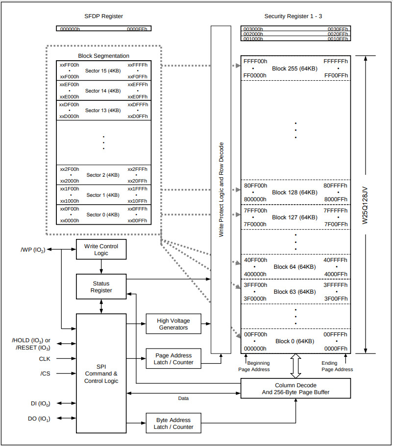
In flash particles, byte is the smallest reading unit and supports random reading. For writing operations, it is more complicated. If you want to write 0 , you only need to program the corresponding storage unit. If we write 1 , we must first perform an erase operation. Due to the physical features of the flash memory unit, the sector is the smallest eraser. That is, we need to read out all the storage contents of the sector and then erase the sector. And then program the sector according to the new data. It can be seen that the writing overhead of flash is much greater than that of reading.
In addition to the storage array, flash particles also contain several registers, including some address registers used to control the address of reading and writing flash particles, control registers used to control the behavior of the particles (such as write protection, access permissions, etc.), and status registers used to store the current reading and writing status of the flash particle. As you can see, the inside of the flash particle is a device controller!
In order to access the flash particle, an external command needs to be sent to. After the flash particle receives the external command, it will parse the command and then execute the specific function of the command. This is very similar to the process of the CPU executing instructions. The CPU instruction cycle includes fetching, decoding, executing, and updating the PC. For most devices, including flash particles, the processing process includes receiving commands, parsing, executing, and waiting for new commands. As for the format and function of the command, it is defined by the corresponding manual . For example, the 8-bit command 03h means reading data from the flash particle, and the command is followed by the 24-bit storage unit address. Therefore, if you have learned CPU design, you are fully capable of designing the core logic of flash particles according to the design manual of it.
With the help of the bus, we can easily translate the CPU's memory access request into the read and write commands of the flash particles. Taking the load request whose target address is the flash space as an example, when the CPU's LSU executes the load instruction, it will initiate a read transaction on the bus , the read transaction passes through The command is sent to the flash particle. After a period of time, the flash controller obtains the data read from the flash particle and transmits the data to the CPU as a reply to the bus transaction. After the CPU's LSU receives the read result, the load instruction continues to execute.
RTFSC to understand the process of reading data from flash
ysyxSoC contains the code implementation of the above process, and maps the flash storage space to the CPU's address space 0x3000_0000~0x3fff_ffff . You need to first define the macro FAST_FLASH in ysyxSoC/perip/spi/rtl/spi_top_apb.v , and then try to understand the above in combination with the code process.
Regarding the writing to flash, because writing to flash requires erasing an entire sector before rewriting the whole set of data, it is necessary to send multiple commands to the flash chip. However, at present, we are only looking to use flash to replace MROM, so that NPC can fetch valid instructions from the flash upon reset. Therefore, we will not be performing write operations on the flash chip for the time being. The flash chip code in ysyxSoc also only supports read operations.
Read data from flash
After understanding the process of reading data from flash, you can then test this process through code:
- Define an array representing the flash storage space in the simulation environment
- When the simulation environment is initialized, write certain contents to the above array.
- This operation can be seen as simulating the process of programming data into flash particles.
- Correctly implement
flash_read()function so that it returns the content of the corresponding location in flash according to the parameteraddr. - Write a simple test program in
am-kernels, read the content from the flash storage space, and check whether it is consistent with the content set when the simulation environment is initialized.
Access flash particles through SPI bus protocol
Due to the manufacturing process of flash chips being different from that of processor chips, the processor and flash chips must be manufactured separately and then soldered onto a board, where they communicate through the wires on the board. For this reason, the number of pins becomes a consideration. On one hand, if there are too many pins, it is not conducive to minimizing the size of the chip, which can negatively affect the layout and area of the board. On the other hand, the wires on the board are usually longer than those inside the chip, making the signals more susceptible to interference. Consequently, a high number of pins can lead to a dense arrangement of traces on the board, where these traces can easily interfere with each other, affecting the stability of the signals.
Taking the read command mentioned above as an example, a read operation involves at least an 8-bit command, a 24-bit address, and an 8-bit data, which already occupies a 40-bit signal. Therefore, all these signals are passed through the pins. Going outside the flash particle is not a good solution.
In order to reduce the number of pins of the flash particle, an SPI bus interface is generally added to the flash particle. The full name of SPI is Serial Peripheral Interface, which is a serial bus protocol that is carried out between the master and the slave through a few signal lines for communication.
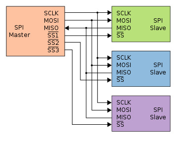
There are only 4 signals in total on the SPI bus:
SCK- the clock signal sent by the master, only 1 bitSS- slave select, the selection signal sent by the master, used to specify the communication object, each slave corresponds to 1 bitMOSI- master output slave input, the data line used by master to communicate with slave, only 1 bitMISO- master input slave output, the data line used by the slave to communicate with the master, only 1 bit
To communicate over the SPI bus, the master usually first selects the target slave with the SS signal, then sends the SPI clock pulses to the slave with the SCK signal, while converting the information to be sent into a serial signal, transmitting it to the slave bit by bit through the MOSI signal; then it listens to the MISO signal, and converts the serial signal received through MISO back into parallel information, thereby obtaining the reply from the slave.
The working mode of the slave is similar, if the slave receives the SCK clock pulses while the SS signal is active, it listens to the MOSI signal, and converts the serial signal received through MOSI into parallel information, thereby obtaining the command sent by the master; after processing the command, it converts the information to be replied into a serial signal, transmitting it to the master bit by bit through the MISO signal.
As we can see, aside from the state machine, the core of implementing the SPI bus protocol lies in the conversion between serial and parallel signals. Specifically, it involves how the sender transmits signals and how the receiver samples and receives them. On one hand, we need to consider the endianness of the transmission: whether it is from most significant bit to least significant bit, or vice versa. On the other hand, we need to consider the timing of transmission and sampling (clock phase): whether it occurs on the rising edge or the falling edge of SCK. Sometimes, the idle state level of the clock (clock polarity) is also defined: whether it is high or low when idle. During the transmission and sampling process, SCK plays a role in synchronization. Both parties agree on the endianness and timing of transmission/sampling and correctly implement the agreement at the RTL level. In real scenarios, different slaves may have different agreements, meaning that when communicating with different slaves, the master needs to adapt to the agreements of the slaves for transmission and sampling.
However, upper-level software does not wish to concern itself with these signal-level behaviors. Therefore, the SPI master also needs to abstract these signal-level behaviors into device registers. By accessing these device registers, the upper-level software can query or control the SPI master. In fact, in the bus architecture, the SPI master has a dual role. On one hand, it acts as a slave to AXI (or other AMBA protocols, such as APB), responsible for receiving commands from the CPU. On the other hand, it serves as the master to SPI, responsible for sending commands to the SPI slaves. Thus, we can also view the SPI master as a bridge module between AXI and SPI, converting AXI requests into SPI requests to communicate with SPI slaves.
The ysyxSoC integrates the implementation of an SPI master, and maps its device registers into the CPU's address space 0x1000_1000~0x1000_1fff, with related code and documentation located in the corresponding subdirectories under ysyxSoC/perip/spi/. With the abstraction of device registers, we can then delineate the behavior of higher-level software. To communicate with different slaves, the master generally needs to support multiple protocols, and the specific setting of which protocol to use is accomplished by configuring the device registers. Before communicating with a slave, the SPI driver first sets the SS register to select the target slave, and configures the SPI master's control registers according to the slave's protocol, then writes the data to be transmitted into the transmission data register, and finally writes a command that signifies "start transmission" into a control register. The SPI driver can poll the SPI master's status register, waiting when the status flag is "busy" and continuing only when the status flag turns to "idle", at which point the slave's response can be read from the reception data register.
Implement the bit flip module based on SPI protocol
To become familiar with and test the basic process of SPI, let's write a simple bit reversal module, bitrev. This module receives an 8-bit data input and then outputs the result of reversing the bits of that data. Specifically, it swaps the 0th bit with the 7th bit, the 1st bit with the 6th bit, and so on.
Specifically, if you choose Verilog, you need to implement the corresponding code within ysyxSoC/perip/bitrev/bitrev.v; if you choose Chisel, you need to implement the corresponding code within the bitrevChisel module in ysyxSoC/soc/BitRev.scala, and modify Module(new bitrev) in ysyxSoC/soc/SoC.scala to instantiate the bitrevChisel module.
If the input and output signals of the bitrev module are 8 bits, then it would be a simple digital circuit assignment. However, since the bitrev module communicates via the SPI bus, you also need to implement the conversion between serial and parallel signals. This task is not difficult; our Chisel reference code only requires adding about 5 lines. Here are some tips:
SSsignal output by the SPI master is active at low level, andMISOsignal is set to high level when the slave is idle.- Since
SCKonly generates pulses during SPI transmission, you may need to use the asynchronous reset function. However, this bitrev module does not participate in tape-out, and using asynchronous reset does not affect the tape-out process.- If you use Chisel, you can refer to the instructions on Reset in the Chisel documentation.
- If you use Chisel and want to use clock falling edge triggering, you can refer to this post
- You also need to cancel the macro
FAST_FLASHdefined inysyxSoC/perip/spi/rtl/spi_top_apb.vso that APB requests can access the device register of the SPI master.
After implementing the bitrev module in hardware, you will also need to write a program to test it. Try writing an AM (Abstract Machine) program that drives the SPI master to input an 8-bit data into the bitrev module and then read out the processed result to check if it meets the expected outcome. Specifically:
- Set the data to be sent to the TX register of the SPI master
- Set the divisor register, which is used to indicate the ratio of
SCKfrequency to the current SPI master clock frequency when the SPI master transmits. Since there is no concept of frequency in verilator, you can set a divisor to make theSCKfrequency as high as possible.- In a real chip, if
SCKfrequency is too high, the slave may not work correctly, so the setting of the divisor register needs to meet the requirements of the slave operating frequency.
- In a real chip, if
- Set
SSregister and select the revbit module as slave- ysyxSoC has connected bitrev as an SPI slave to the SPI master, and its slave number is 7
- Set the control register. Specifically, you need to set each field in it. The description of some of the fields is as follows:
CHAR_LEN- Since the input and output data are both 8 bits in length, the transfer length should be 16 bitsRx_NEG,Tx_NEGandLSB- Since bitrev is just a test module and does not participate in the final tape-out, we do not stipulate these details of the bitrev module and leave it to you to make an agreement. You need to choose a convention and follow this convention to implement the bitrev module, set the SPI control register and write software so that the three can communicate according to the same conventionIE- Currently we don't use the interrupt functionASS- It can be set or not, but it needs to be considered in conjunction with the software
- Poll the completion flag in the control register until the SPI master completes the data transfer
- Read the data returned by slave from the RX register of SPI master
We give an example of a data transfer. Note that this is just a schematic diagram, and your implementation does not have to be exactly the same:
                +---+   +---+   +---+   +---+   +---+   +---+   +---+   +---+   +---+   +---+   +---+   +---+   +---+   +---+   +---+   +---+
 SCK            |   |   |   |   |   |   |   |   |   |   |   |   |   |   |   |   |   |   |   |   |   |   |   |   |   |   |   |   |   |   |   |
        --------+   +---+   +---+   +---+   +---+   +---+   +---+   +---+   +---+   +---+   +---+   +---+   +---+   +---+   +---+   +---+   +------------
        --------+                                                                                                                               +--------
 SS             |                                                                                                                               |
                +-------------------------------------------------------------------------------------------------------------------------------+
        +-------+-------+-------+-------+-------+-------+-------+-------+-------+------------------------------------------------------------------------
MOSI            |   b7  |   b6  |   b5  |   b4  |   b3  |   b2  |   b1  |   b0  |
                +-------+-------+-------+-------+-------+-------+-------+-------+
        +-----------------------------------------------------------------------+-------+-------+-------+-------+-------+-------+-------+-------+--------
MISO                                                                            |   b0  |   b1  |   b2  |   b3  |   b4  |   b5  |   b6  |   b7  |
                                                                                +-------+-------+-------+-------+-------+-------+-------+-------+
There are many details in the SPI transmission process, and you will most likely need RTFM and RTFSC to help you understand the details.
Read data from flash through SPI bus
To write an AM program that includes a function prototype uint32_t flash_read(uint32_t addr), it's important to note that this flash_read() function differs from the DPI-C interface function of the same name mentioned earlier. The flash_read() function in this context reads the 32-bit content starting from the address addr in the flash chip by driving the SPI master. The process is similar to the bitrev example mentioned earlier, with the following steps:
- Set the command that needs to be sent to the flash particle into the TX register of the SPI master
- Set the divisor register
- Set the
SSregister, select the flash particle as the slave, and its slave number is 0 - Set control register:
CHAR_LEN- Since the length of the read command is 32 bits and 32 bits of data need to be read, the transmission length should be 64 bits.Rx_NEGandTx_NEG- need to be set according to the slave's relevant documents- In real chip designs, incorrect settings of
Rx_NEGandTx_NEGcan lead to violations of the hold time requirements during circuit operation, resulting in incorrect data sampling. However, Verilator does not simulate timing, so some incorrect settings might still produce correct results in simulation. Nevertheless, it is still recommended to strictly follow the conventions after RTFM to set these parameters correctly.
- In real chip designs, incorrect settings of
LSB- needs to be set according to the relevant documentation of the slave. If necessary, the tail end of the read data can be adjusted through softwareIE- Currently we don't use the interrupt functionASS- It can be set or not, but it needs to be considered in conjunction with the software
- Poll the completion flag in the control register until the SPI master completes the data transfer
- Read the data returned by slave from the RX register of SPI master After implementing
flash_read(), use this function to read the content from the flash storage space and check whether it is consistent with the content set when the simulation environment is initialized.
Load the program from flash and execute it
Try to store char-test program mentioned above into the flash particle, write a test program, read char-test from flash to an address in SRAM through flash_read() , and then jump to the address to execute char-test .
Fetch instructions from flash
After the data can be read correctly from the flash, we can consider putting the program that needs to be executed into the flash and let the NPC retrieve the first instruction from the flash.
Wait a minute, something seems off... We just used the function flash_read() to read content from flash, and this function is also part of the program. It is compiled into an instruction sequence and stored in MROM, with the NPC fetching and executing instructions from MROM. But if the instruction sequence for flash_read() is also programmed into the flash, who will fetch and execute the instructions for flash_read()? This turns into a "chicken and egg" circular dependency problem.
Upon further analysis, the root of the problem is that we are attempting to implement instruction fetching, which is inherently a hardware-level behavior, through a software function. This approach is fundamentally flawed because instruction fetching is a hardware-level operation. Therefore, we should aim to implement the functionality of "fetching instructions from flash" at the hardware level.
To implement the functionality of flash_read() at the hardware level means accessing the registers of the SPI master in a certain sequence on the hardware. As you may have thought, this can be achieved using a state machine to implement the flash_read() functionality! Unlike the method described earlier, where the program is loaded from flash and executed, this approach of fetching instructions directly from the flash chip does not require the program to be read into memory (corresponding to the SRAM mentioned earlier) before execution. Therefore, this method is also known as "execute in place" (XIP).
To differentiate from the normal access to the SPI master, we need to map the functionality of accessing flash through XIP to a different address space from that of the SPI master device registers. In fact, we can slightly adjust the previously accessed flash storage space 0x3000_0000~0x3fff_ffff and define it as the flash storage space accessed through XIP. In the ysyxSoC, the Xbar has already mapped both the address space of the SPI master 0x1000_1000~0x1000_1fff and the flash storage space 0x3000_0000~0x3fff_ffff to the APB port in the ysyxSoC/perip/spi/rtl/spi_top_apb.v module. That is, the APB port in the spi_top_apb.v module can receive requests from the aforementioned two address spaces, and you can distinguish them by checking the target address of the APB.
Access flash through XIP
To sum up, the general process of implementing the XIP method is as follows:
- Check the target address of the APB request. If the target address falls in the address space of the SPI master, access and reply normally.
- If the target address falls in the flash storage space, it enters XIP mode. In XIP mode, the input signal of the SPI master is determined by the corresponding state machine
- The state machine writes corresponding values to the device register of the SPI master in turn. The written values are basically the same as
flash_read() - The state machine polls the completion flag of the SPI master and waits for the SPI master to complete the data transmission.
- The state machine reads the data returned by flash from the RX register of the SPI master, returns it through APB after processing, and exits XIP mode
- The state machine writes corresponding values to the device register of the SPI master in turn. The written values are basically the same as
Specifically, if you choose Verilog, you need to implement the corresponding code in ysyxSoC/perip/spi/rtl/spi_top_apb.v ; if you choose Chisel, you need to implement the corresponding code in Impl class of ysyxSoC/soc/SPI.scala .
Before fetching instructions via XIP, it's crucial to test if the CPU can successfully complete read requests through XIP. You can write a test program that directly reads content from the flash storage space via a pointer and checks if it matches the content set during the initialization of the simulation environment. Here's a basic outline of steps to follow for writing such a test program:
Similarly, we currently do not consider supporting flash write operations through XIP, so you'd better find a way to report an error when a write operation is detected to help you diagnose the cause of the problem in time.
Execute the program in flash through XIP
Store char-test program mentioned above in the flash particle, write the test program, and jump to the flash to execute char-test .
Use flash instead of MROM
After confirming that instructions can be successfully fetched and executed directly from flash, it's feasible to entirely replace the MROM with flash for storing the first program. This involves modifying the reset value of the PC so that upon reset, the NPC fetches the first instruction from flash. Adapting to this change requires a series of modifications. Making these changes requires a thorough understanding of the system's architecture, including how the CPU interacts with memory and peripheral devices. It also tests your knowledge
Because the size of flash is much larger than the MROM used previously, we are now able to store and execute larger programs, such as attempting to run programs that include printf() like coremark. If you run microbench, you will find that numerous sub-items fail to execute due to insufficient heap size.
coremark takes a long time to run
If you were allowed to do it, how would you reduce coremark's running time?
Hint: RTFSC
Try to execute flash_read() function on flash
You may find an error, please try to analyze why this error occurs.
Add student ID CSR and output student ID
To identify different students' NPCs, we can set our own student ID in the CSR identification registers. Specifically, you can add the following two CSRs in the NPC:
mvendorid- Read the ASCII code ofysyxfrom it, which is0x79737978marchid- Read out the decimal representation of the numeric part of the student number. Suppose your student number isysyx_22068888, then read22068888, which is0x150be98
After implementation, the values of the above two CSRs can be read and output before the TRM of riscv32e-ysyxsoc enters main() function.
wait for SPI master transfer to complete via interrupt
Our recent implementation of XIP continuously polls to check if the SPI master's transmission is complete. In fact, the SPI master also supports an interrupt notification mode. After setting the IE bit in the control register, the SPI master will issue an interrupt signal once the transmission is finished. The state machine in XIP mode can wait for this interrupt signal to wait for the SPI master transmission to complete. Students interested in this can implement the above-mentioned interrupt querying method.
Although this does not bring a significant performance improvement, in actual systems, waiting for interrupts can save energy because the requests and responses initiated by polling do not make a real contribution to the system's operation.
Random access memory with higher storage density
After resolving the issue of MROM only being able to store small programs with flash, we also need to consider data storage. If a program needs to write an amount of data exceeding the 8KB provided by SRAM, then the program still cannot run on the ysyxSoC. Therefore, we need a larger storage that can also support the CPU executing store instructions.
DRAM memory unit
DRAM (Dynamic Random Access Memory) is a widely used type of memory, which, compared to SRAM, features larger capacity and lower cost. The storage cell of DRAM stores 1 bit of information using a transistor and a capacitor. The transistor acts as a switch, serving the function of read/write enable, while the capacitor is used to store the 1 bit of information. When the charge of the capacitor is above a certain threshold, it is considered a 1; otherwise, it is considered a 0. Thus, DRAM stores information based on the properties of electricity, making it a volatile memory; all information stored in DRAM is lost when power is removed. Conversely, when the system is powered on, there is no valid data in DRAM.
However, capacitors exhibit the characteristic of leakage. If left unattended, the charge within the capacitor will progressively diminish, ultimately reaching zero. This renders it impossible to discern whether the original stored data was a 1 or a 0, leading to data loss. To circumvent this issue, it is essential to periodically refresh the storage cells in DRAM:
- The DRAM controller reads the information contained in each storage cell. If it is a
1, then it rewrites this information into the same storage cell. - The rewrite operation replenishes the capacitor in the storage cell to a high charge state, ensuring that a
1can be read from the cell over the following period, thereby preserving the stored information.
As can be seen, writing to a DRAM storage cell fundamentally involves charging and discharging a capacitor. Therefore, although the write operations to DRAM are not as fast as those to SRAM, when considering factors such as cost and capacity, DRAM's write operations are still suitable for supporting CPU execution of store instructions.
If we disregard the organizational structure of the storage array and the physical process of reading and writing, functionally, DRAM chips are very similar to the flash chips described earlier: besides various registers, they can also receive external input commands to operate.
Similar to a flash controller, the module that sends commands to DRAM chips to drive their operation is called a DRAM controller. The DRAM controller needs to translate transaction requests from the bus into operational commands for the DRAM chips, passing this information to the DRAM chips via the memory bus. Additionally, the DRAM controller must also periodically send refresh commands to the DRAM chips. However, this also increases the design complexity of the DRAM controller: it must precisely calculate the timing for refreshes. Too many refresh operations can reduce the efficiency of read and write command execution, while too few refresh operations can lead to data loss.
PSRAM particles
There's a type of DRAM chip that integrates the logic for refresh internally, known as PSRAM (Pseudo Static Random Access Memory) chips. A PSRAM controller does not need to implement the refresh function, nor does it need to be concerned with the internal structure of PSRAM chips. Therefore, using these chips is very similar to using SRAM: one simply needs to provide the address, data, and read/write commands to access data within the chip. An example is the IS66WVS4M8ALL PSRAM chip, which provides 4MB of storage space. For more information, you can refer to the relevant manuals.
With PSRAM, we can attempt to provide a larger writable memory area for programs in the ysyxSoC. Similar to accessing flash chips via the SPI protocol, PSRAM chips also offer an SPI interface. However, unlike flash, PSRAM generally serves as the system's memory, necessitating a more efficient access method.
Access PSRAM particles through an upgraded version of the SPI bus protocol
In fact, there are some upgraded versions of the SPI protocol that can enhance the communication efficiency between the master and the slave. The basic SPI protocol is full-duplex, meaning that the master and the slave can simultaneously send messages through MOSI and MISO respectively. However, usually, the master sends a command to the slave first, and the slave can only process this after receiving the command, and then it can reply to the master with the result. This process only requires a half-duplex channel.
The Dual SPI protocol takes advantage of this, allowing the basic SPI protocol's MOSI and MISO to be used for transmission in one direction simultaneously, i.e., the Dual SPI protocol can transmit 2 bits in one direction within a single SCK clock cycle. Because the meanings of MOSI and MISO have changed, in the Dual SPI protocol, their names are changed to SIO0 (Serial I/O 0) and SIO1 respectively.
To distinguish from the transmission method of the basic SPI protocol, the slave usually offers different commands to allow the master to choose which protocol to use for transmission. For example, the flash chip model W25Q128JV mentioned above provides multiple read commands:
- The
03hcommand is provided for read operations using the basic SPI protocol, with the command, address, and data all transmitted at 1 bit per transfer. The transmission bit width of these three components is usually represented by a triplet(command transmission bit width - address transmission bit width - data transmission bit width), for instance, the basic SPI protocol is also denoted as(1-1-1). Taking the reading of 32 bits of data as an example, the03hcommand requires8 + 24 + 32 = 64SCKclock cycles to execute. - The
3Bhcommand is also provided, utilizing the Dual SPI protocol for read operations. Its command and address are transmitted in 1 bit, while the data is transmitted in 2 bits, denoted as(1-1-2). Taking the example of reading 32 bits of data, the3Bhcommand requires8 + 24 + 32/2 = 48SCKclocks to execute. However, irrespective of the number of bits used for data transmission, there is always a certain delay in reading data from the flash memory array. Hence, before transmitting data, the3Bhcommand also needs to wait for an additional 8SCKclocks, meaning that the3Bhcommand requires8 + 24 + 8 (read delay) + 32/2 = 56SCKclocks to execute. - The
BBhcommand is also provided, utilizing the Dual SPI protocol for read operations. Its command is transmitted in 1 bit, while the address and data are transmitted in 2 bits, denoted as(1-2-2). Taking the example of reading 32 bits of data, theBBhcommand requires8 + 24/2 + 4 (read delay) + 32/2 = 40SCKclocks to execute.
Furthermore, there is the Quad SPI protocol (abbreviated as QSPI), which introduces two additional signals, SIO2 and SIO3, enabling the unidirectional transmission of 4 bits within a single SCK clock cycle. For example, the flash chip model W25Q128JV mentioned earlier also provides two additional read commands based on the QSPI protocol:
6Bhcommand is provided. The command and address are transmitted in 1 bit, but the data is transmitted in 4 bits, recorded as(1-1-4). Taking reading 32-bit data as an example, the6Bhcommand needs to execute8 + 24 + 8(read delay) + 32/4 = 48SCKclocks.- Also provided is the
EBhcommand, where the command is transmitted in 1 bit, but the address and data are transmitted in 4 bits, denoted as(1-4-4). Taking the example of reading 32 bits of data, theEBhcommand needs to execute8 + 24/4 + 6 (read delay) + 32/4 = 28SCKclocks.
However, in the above read command, regardless of how many bits the address and data parts are transmitted in, the command part is always transmitted in 1 bit. This is because the slave, after decoding the command, determines the subsequent address and data transmission protocols. Therefore, the command part still follows the basic SPI protocol for bit-by-bit transmission. Additionally, although the flash chips of the mentioned model support multiple transmission modes, the SPI master connected to the flash chips can only transmit using the basic SPI protocol, thus unable to issue other read commands.
The ysyxSoC integrates an implementation of a PSRAM controller and maps the PSRAM storage space to the CPU's address space 0x8000_0000~0x9fff_ffff. The code for the PSRAM controller is located in the directory ysyxSoC/perip/psram/efabless/, which uses the Wishbone bus protocol. We have encapsulated it into the APB bus protocol (see ysyxSoC/perip/psram/psram_top_apb.v) and connected it to the APB Xbar of ysyxSoC. The PSRAM controller translates received bus transactions into commands sent to the PSRAM chip. We have chosen the IS66WVS4M8ALL PSRAM chip for simulation, which supports the QSPI protocol. Therefore, the PSRAM controller integrated into ysyxSoC can communicate with the PSRAM chip using the QSPI protocol, allowing more efficient access to the PSRAM through commands. The ysyxSoC has already connected the PSRAM chip to the PSRAM controller but has not provided code related to the PSRAM chip. To use the PSRAM in ysyxSoC, you will need to implement a behavioral model for the PSRAM chip.
Implement the simulation behavior model of PSRAM particles
You need to implement a behavioral model for the IS66WVS4M8ALL chip. You only need to implement two commands in SPI mode: Quad IO Read and Quad IO Write. Their command encodings are EBh and 38h respectively. The PSRAM controller will only send these two commands to the PSRAM chip.
Specifically, if you choose Verilog, you need to implement the corresponding code in ysyxSoC/perip/psram/psram.v. If you choose Chisel, you need to implement the corresponding code in the psramChisel module in ysyxSoC/soc/PSRAM.scala, and modify Module(new psram) in ysyxSoC/soc/SoC.scala to instantiate the psramChisel module.
Some instructions are as follows:
- The meaning of port
ce_nis the same asSSin the SPI bus protocol, low level is active - The port
diois declared as aninouttype, and coupled with an output enable signal, it can realize three-state logic. It can be used for input or output at the same time to achieve half-duplex transmission of signals.- In the ASIC process, it is necessary to explicitly instantiate the three-state logic unit in the standard unit library, but here we are only testing in the simulation environment, so there is no need to call the standard unit library
- If you use Verilog, you can refer to the relevant code of
qspi_dioinysyxSoC/perip/psram/psram_top_apb.v - If you use Chisel, since Chisel currently does not support other operations of
Analogtype except connection, we have instantiated aTriStateBufsubmodule in the framework code, which can decomposediointoUIntsignals in both directions ofdinanddoutfor subsequent use
- The storage array only needs to be implemented as a two-dimensional array with a word length of 8 bits. There's no need to concern yourself with its physical organization; the focus should be on implementing the QSPI protocol. Additionally, since PSRAM is not non-volatile memory, there's no need to initialize its contents in the simulation environment. Therefore, you can directly define the storage array in Verilog code or access an array defined in C++ code through DPI-C, making it easier to trace with mtrace.
- There is also a QPI Mode in the manual, which has a different meaning from the QSPI mentioned above and can be ignored for now.
- For details such as tail end and clock phase, please refer to the relevant manual for RTFM, or refer to the PSRAM controller code for RTFSC.
- In order to correctly implement communication between the PSRAM controller and PSRAM particles, you do not need to modify the code of the PSRAM controller
After implementation, test a small segment of PSRAM access (such as 4KB) using mem-test to check if your implementation is correct. Note that the flash already provides a larger storage space for storing programs. Therefore, you can use printf() in mem-test to help you output debugging information, especially information related to the progress of the test, to ensure that the test is proceeding normally.
In fact, there is a protocol called QPI on top of QSPI, which can further enhance the efficiency of the command transfer. In QPI protocol, commands, addresses, and data are all transmitted in 4-bit chunks, denoted as (4-4-4). However, to maintain compatibility with old SPI masters, slaves typically start in basic SPI mode when powered on, communicating via the basic SPI protocol at that time. If the slave supports the QPI protocol, it will provide a command to switch to QPI mode. The master can send this command to switch the slave to QPI mode and then communicate with it using the QPI protocol.
Use QPI protocol to access PSRAM particles
Try adding QPI mode support to the PSRAM chips and defining the command to enter QPI mode. Then, modify the code of the PSRAM controller so that after resetting, it first sends the command to enter QPI mode to the PSRAM chips via circuit logic. Subsequently, communication with the PSRAM chips should be done in QPI mode.
Note that the addition of this function is transparent to the upper-layer software. The upper-layer software does not need to make any changes to improve the efficiency of accessing PSRAM.
Run larger programs
With the support of PSRAM, we can try to allocate data segments in PSRAM to support running larger programs.
Run microbench on ysyxSoC
Previously, we allocated the data segment and heap in an 8KB SRAM, but the memory required to run the microbenchmark exceeds 8KB, causing many subtests to be unable to run. By allocating the data segment and heap in a 4MB PSRAM instead, you should be able to see the successful execution of all test cases in the microbenchmark at test scale.
We just ran microbench to demonstrate the allocation of data segments in PSRAM has no major issues in the process. However, before running more programs, it is better to perform a comprehensive test on the 4MB PSRAM using mem-test. Nevertheless, testing the read and write of this 4MB memory space completely through mem-test in a simulated environment would take a long time.
This is because currently we are running mem-test in flash: fetching an instruction from flash requires at least 64 SCK clock cycles; and the SPI master generates SCK clock signal through division, even with the most efficient halving, just the SPI transfer process takes at least 128 CPU clock cycles; adding the overhead of the XIP state machine control, fetching an instruction from flash would require approximately 150 CPU clock cycles in total.
Due to the existence of loops and function calls, most of the code in the program needs to be repeatedly executed. Instead of running the program continuously in flash, spending some time upfront to load the code into a storage with higher access efficiency than flash, and then executing the program repetitively in the latter, can effectively improve the program's execution efficiency. However, this loading process requires reading the program instructions and then writing them into the target storage, hence necessitating a storage that supports write operations. Currently, PSRAM is still under testing, considering mem-test is not very large, we can attempt to load mem-test into the 8KB SRAM mentioned above.
Who will perform this loading operation? We certainly need to complete the loading before executing mem-test, but we also want to maintain the feature of "fetching instructions from flash after NPC reset", minimizing interference in the simulation environment and enabling this loading operation to be carried out on the actual chip. Therefore, we have no choice but to utilize the gap after NPC reset and before the actual execution of mem-test for loading, and it is not difficult to realize that this can be achieved through the bootloader! In other words, we need to extend the functionality of the bootloader to load all of the program's code and data into SRAM, and then jump to execute from SRAM.
Completely test PSRAM access
Expand the function of bootloader, completely load mem-test into SRAM, and then execute mem-test . Some tips are as follows:
- You also need to load the read-only data segment into SRAM, which may contain some data required for code execution, such as jump tables, etc.
- If you find that
mem-testhas too much code to fit in SRAM, you can try using the compile option-Osto instruct gcc to optimize based on code size. - The implementation of code loading also needs to deal with some details that you can understand now. If you ignore them, then learn it during debugging. After all, the same will be true for real projects in the future.
After that, let mem-test test all 4MB storage space of PSRAM. You will find that the running efficiency of mem-test has improved a lot, and it can take about 10 minutes to complete the test.
Although SRAM has fast access speed, its capacity is limited and cannot store most programs. After completing the full test of PSRAM access, we can also consider having the bootloader load the program entirely into PSRAM to enhance the program execution efficiency.
Load the program into PSRAM through bootloader for execution
Since you have already loaded mem-test into SRAM through the bootloader, loading the program into PSRAM should not be difficult. However, to fully utilize SRAM, allocating the stack in SRAM can enhance the efficiency of function calls and accessing local variables.
When attempting to run the microbench test, you will notice a significant performance improvement by loading it into PSRAM and executing it compared to running it in flash.
Execute RT-Thread on PSRAM
The current capacity of PSRAM is enough to run RT-Thread. Try to load RT-Thread into PSRAM through bootloader for execution.
If the program is large, the process of the bootloader loading the program will also take longer because the bootloader itself runs in flash. Similarly, can we load the code for "bootloader loading program" into a storage with higher access efficiency first, and then execute the functionality of "bootloader loading program"? This is essentially a multi-stage loading process of the bootloader. For ease of distinction, we can divide the entire bootloader's work into two parts: FSBL (First Stage Bootloader) and SSBL (Second Stage Bootloader). Upon system power-up, FSBL, SSBL, and the program to be run are all located in flash; FSBL is the first to execute, responsible for loading SSBL from flash to other storage, and then jumping to execute SSBL; SSBL is responsible for loading the subsequent program to run from flash into PSRAM, and then jumping to the program and executing it. In fact, the code for SSBL is not large, so we can have FSBL load SSBL into SRAM for faster execution.
implements the secondary loading process of bootloader
Implement FSBL and SSBL according to the above functions. In order to know the scope of SSBL in flash, you may need to put SSBL in a separate section. For details, please refer to the relevant code in start.S .
In addition, because the bootloader divides the loading work into multiple stages, you need to additionally consider whether the target object is accessible in the current stage.
Internal structure of SDRAM particles
If you want to further enhance the efficiency of accessing DRAM chips, you should consider changing the serial bus between the controller and the chips to a parallel bus. For example, the internal structure of a DRAM chip with the model MT48LC16M16A2 is illustrated in the diagram below. This chip has 39 pins, which include:
CLK,CKE- clock signal and clock enable signalCS#,WE#,CAS#,#RAS- Command signalsBA[1:0]- memory bank addressA[12:0]- addressDQ[15:0]- dataDQM[1:0]- data mask, the naming in the figure below usesDQMLandDQMH
Different from the frequency-divided SCK used in the SPI protocol, the clock signal CLK here is usually directly driven by the clock of the DRAM controller. Such type of DRAM is called Synchronous DRAM, known as SDRAM (Synchronous Dynamic Random Access Memory). SDRAM chips have become the mainstream memory chips currently. The earliest commercially available SDRAM chips were introduced in 1992, belonging to SDR SDRAM (Single Data Rate SDRAM), where one data transfer occurs per clock cycle. The chip model shown in the diagram, MT48LC16M16A2, is an example of an SDR SDRAM chip. DDR SDRAM (Double Data Rate SDRAM) emerged in 1997, which can transfer data on both the rising and falling edges of the clock signal, thereby improving data transfer bandwidth. Subsequently, DDR2, DDR3, DDR4, and DDR5 were introduced, each enhancing data transfer bandwidth through different technologies. In contrast to Synchronous DRAM, there is also Asynchronous DRAM (Asynchronous DRAM), which does not have a clock signal in its bus. Currently, Asynchronous DRAM is mostly replaced by SDRAM, so when discussing DRAM today, it almost exclusively refers to SDRAM.
Unlike the SPI bus interface of PSRAM chips, the pins of traditional DRAM chips contain information such as memory cell addresses. This requirement necessitates that the DRAM controller understands the internal organization structure of the memory array in the DRAM chip to know what information to pass to the pins related to addresses.
The memory array of a DRAM chip is a multi-dimensional structure, logically composed of several matrices, where each matrix is also known as a memory bank. Each matrix in a memory bank consists of several memory cells, with each cell containing a transistor and a capacitor used to store 1 bit of information. To specify a matrix element in a memory bank, both a row address and a column address are required. For example, in the aforementioned DRAM chip, there are 4 memory banks, each with 8192 rows and 512 columns. Each matrix element in a memory bank contains 16 memory cells. Therefore, the capacity of this DRAM chip is calculated as 4 * 8192 * 512 * 16 = 256Mb = 32MB.``
During a read operation, a target memory bank is first selected based on the bank number. Subsequently, a row address is used to activate a row in the target memory bank: the sense amplifier in the target memory bank detects the charge levels in all memory cells of that row, determining whether each cell stores a 1 or 0. A sense amplifier is typically composed of a pair of cross-coupled inverters, allowing it to store information; thus, the sense amplifier in the memory bank is also known as a row buffer, capable of storing a row of information. Following this, data is selected from the row buffer of the target memory bank based on the column address and is output as the read result from the DRAM chip to the external interface.
During a write operation, the data to be written is first stored in the appropriate location in the row buffer. Subsequently, the capacitors in the corresponding memory cells are charged or discharged to transfer the contents of the row buffer to the memory cells. If access to data from another row is required, before activating the new row, the information from the currently activated row needs to be written back to the memory cells, a process known as precharging.
Physical implementation of DRAM particles
Considering the limitations of physical implementation, long interconnections can introduce significant delays. Therefore, from a physical implementation perspective, a memory bank in a DRAM chip is further divided into multiple subarrays. However, the structure and access methods of these subarrays are transparent to the external interface of the chip; the DRAM controller does not need to be concerned with them when sending commands to the DRAM chip. Students interested in this topic can read this article to further understand the physical structure inside a DRAM chip.
After understanding the internal organization of DRAM chips, we can then proceed to outline the commands for DRAM chips. The commands for different versions of SDRAM vary slightly. The table below lists the commands for SDR SDRAM:
| CS# | RAS# | CAS# | WE# | Command | Meaning |
|---|---|---|---|---|---|
| 1 | X | X | X | COMMAND INHIBIT | Nothing |
| 0 | 1 | 1 | 1 | NO OPERATION | NOP |
| 0 | 0 | 1 | 1 | ACTIVE | Activate a row in the target memory bank |
| 0 | 1 | 0 | 1 | READ | Read a column from the target memory bank |
| 0 | 1 | 0 | 0 | WRITE | Write a column in the target memory bank |
| 0 | 1 | 1 | 0 | BURST TERMINATE | Stop the current burst transfer |
| 0 | 0 | 1 | 0 | PRECHARGE | Close the activated row in the memory bank (precharge) |
| 0 | 0 | 0 | 1 | AUTO REFRESH | refresh |
| 0 | 0 | 0 | 0 | LOAD MODE REGISTER | Set Mode register |
The above commands involve the concept of "burst transfer," which refers to including multiple consecutive data transfers in a single transaction, with each data transfer being called a "beat." Taking reading as an example, when a READ command is received from the DRAM chip, it usually takes several cycles to read the data from the storage array and transmit it to DQ bus. This delay is known as CAS latency (some textbooks translate it as CAS latent period).
Using the example of the MT48LC16M16A2 model mentioned earlier, depending on the operating frequency, the CAS latency can range from 1 to 3 cycles. This means that from receiving the READ command to reading out 16 bit data to DQ bus, there is a delay of 1 to 3 cycles.
Assuming a CAS latency of 2 cycles, if burst transfer is not used, reading out 8 bytes would require 12 cycles; whereas with burst transfer, it would only need 6 cycles.
// normal
  1   1   1   1   1   1   1   1   1   1   1   1
|---|---|---|---|---|---|---|---|---|---|---|---|
  ^       |   ^       |   ^       |   ^       |
  |       v   |       v   |       v   |       v
 READ   data READ   data READ   data READ   data

// burst
  1   1   1   1   1   1
|---|---|---|---|---|---|
  ^       |   |   |   |
  |       v   v   v   v
 READ    1st 2nd 3rd 4th
The WRITE command also supports burst transfer, meaning that to write 8 bytes, the data to be written can be continuously transmitted within the following 3 cycles after issuing the WRITE command. As for how many beats are included in a burst transfer transaction, this can be set through the Mode register. The Mode register can also set parameters such as CAS latency.
ysyxSoC integrates the implementation of an SDR SDRAM controller (referred to as the SDRAM controller below) and maps the SDRAM storage space to the CPU's address space 0xa000_0000~0xbfff_ffff. The code for the SDRAM controller is located in the directory ysyxSoC/perip/sdram/core_sdram_axi4/, and it uses the AXI4 bus protocol. For ease of initial testing, we encapsulate its core part ysyxSoC/perip/sdram/core_sdram_axi4/sdram_axi4_core.v into the APB bus protocol (see ysyxSoC/perip/sdram/sdram_top_apb.v), and connect it to the APB Xbar of ysyxSoC.
The SDRAM controller translates received bus transactions into commands sent to the SDRAM chip. We have chosen to simulate the model for the SDRAM chip as the MT48LC16M16A2. While the ysyxSoC has connected the SDRAM chip to the SDRAM controller, it does not provide the code related to the SDRAM chip. Therefore, to use SDRAM in ysyxSoC, you will also need to implement a simulation behavior model for the SDRAM chip.
bug fix
We fixed an issue where the SDRAM controller read request reply was incorrect under certain circumstances. If you obtained the code for ysyxSoC before 2024/02/04 18:00:00, please obtain the new version of the code:
cd ysyxSoC
git pull origin ysyx6
Implement the simulation behavior model of SDRAM particles
You need to implement a simulation behavior model for the MT48LC16M16A2 chip. Specifically, you need to implement the commands that the SDRAM controller will send. The PRECHARGE and AUTO REFRESH commands are related to the electrical characteristics of the memory cells and do not need to be considered in the simulation environment, so they can be implemented as NOP (no operation). Additionally, the Mode register only needs to implement CAS Latency and Burst Length; other fields can be ignored.
Specifically, if you choose Verilog, you need to implement the corresponding code in ysyxSoC/perip/sdram/sdram.v ; if you choose Chisel, you need to implement the corresponding code in the sdramChisel module of ysyxSoC/soc/SDRAM.scala , and Module(new sdram) in ysyxSoC/soc/SoC.scala is modified to instantiate the sdramChisel module.
For other details, please refer to the relevant manual for RTFM, or refer to the code of the SDRAM controller for RTFSC. In order to correctly implement the communication between the SDRAM controller and the SDRAM particles, you do not need to modify the code of the SDRAM controller.
After implementation, test access to a small section of SDRAM (such as 4KB) through mem-test to check whether your implementation is correct.
Completely test SDRAM access
Before further loading the program into SDRAM for execution, we first test access to all storage spaces of the above SDRAM particles through mem-test . It takes about 1 hour to complete this test.
Load the program into SDRAM for execution
Let the bootloader load the program into SDRAM and execute it. After this, try to execute microbench and RT-Thread on SDRAM.
Extension of SDRAM particles
As mentioned earlier, the capacity of the SDR SDRAM chip model MT48LC16M16A2 is 32MB. However, modern memory modules often have capacities of 4GB or more. How is this achieved? Even though contemporary memory modules use more advanced technologies and individual memory chips have higher capacities, it is not solely based on a single memory chip to reach 4GB. In reality, this is accomplished through combining and expanding multiple memory chips in certain dimensions.
If you have observed the structure of a memory module, you will notice that there are multiple memory chips on one module. The memory module itself is a specialized PCB: it integrates multiple memory chips within standard size specifications and uses a DIMM interface, allowing it to be inserted into the memory slots on a motherboard.
We know that, if we disregard the physical organization, memory can be viewed as a two-dimensional matrix where each row stores a word, and the row number represents the address. From this perspective, the extension of multiple chips essentially involves extending in two dimensions: one dimension is to store more bits of information at a single address, known as bit extension; the other dimension is to increase the range of addresses, known as word extension.
The concept of bit extension involves multiple chips simultaneously reading data from the same address. This not only increases the capacity of the memory but also enhances the memory bandwidth. If the word length of the chip (the width of the DQ signal) is smaller than the data width of the bus, bit extension can significantly improve the efficiency of data transfer. For example, for a 64-bit CPU with a bus data width typically not less than 64 bits, using four chips with a word length of 16 bits like the MT48LC16M16A2 chip, it can read out 64 bits after one CAS latency, achieving higher efficiency than burst transfer:
  1   1   1
|---|---|---|
  ^       |
  |       v
 READ   data[15:0]  (chip0)

  1   1   1
|---|---|---|
  ^       |
  |       v
 READ   data[31:16] (chip1)

  1   1   1
|---|---|---|
  ^       |
  |       v
 READ   data[47:32] (chip2)

  1   1   1
|---|---|---|
  ^       |
  |       v
 READ   data[63:48] (chip3)
Another example is the DDR4 SDRAM memory model MTA9ASF51272PZ. The particle word length on the memory stick is 8 bits, but it is bit extended through 8 particles, and 64 bits can be read and written at a time.
Extend the data bit width of the SDRAM controller to 32 bits
Instantiate the submodule of 2 SDRAM particles to simulate the scenario of bit expansion of 2 SDRAM particles. To do this, you need to modify the following:
- Bit width of some signals in SDRAM bus interface
- If you use Chisel, you can directly modify the definition of
SDRAMIO - If you use Verilog, you need to modify the corresponding signal bit width in
ysyxSoC/generated/ysyxSoCFull.v
- If you use Chisel, you can directly modify the definition of
- Internal implementation of SDRAM controller
After implementing bit extension, there is no need to access the SDRAM chips through burst transfer mode. After one CAS latency, it is possible to read out 32 bits of data from the extended chips. You can try running some benchmarks to compare the performance changes before and after bit extension.
However, these performance improvements from bit extension are not free. Bit extension requires a linear increase in the number of DQ pins, which may require careful consideration for cost-conscious chip designs. Additionally, even if cost is not a concern, the performance gains from bit extension can be limited by other factors in the system, such as the data width of the bus. If the maximum data transfer on the bus is limited to 64 bits, then even extending the word length of the memory chips to 512 bits will not yield significant benefits overall, similar to how the flow of water through a pipe is restricted by its narrowest segment.
Another dimension is word extension, where the idea is to distribute different addresses across different chips to increase memory capacity. For example, we can use two 32MB MT48LC16M16A2 chips to form a 64MB memory capacity through word extension. This type of word extension only requires adding 1 address bit on the memory bus, and the increase in pin count is logarithmically related to the storage capacity, resulting in relatively small overhead compared to bit extension. However, intuitively, word extension does not directly increase memory bandwidth, and we will continue discussing this issue in later chapters.
Word expansion for SDRAM controller
Instantiate a submodule consisting of a total of 4 SDRAM chips, where bit extension is applied between two pairs of SDRAM chips, followed by word extension on the results of the bit extension. You will also need to modify the SDRAM bus interface and the internal implementation of the controller accordingly.
After implementation, test all expanded storage spaces through mem-test . It takes several hours to complete this test.
Access more peripherals
All the above work is carried out around TRM. Finally, let's take a look at how to support IOE.
GPIO
First, let's add support for GPIO. GPIO is one of the simplest peripherals, essentially being a wire that connects the inside and outside of the chip, requiring pins on the chip. Through GPIO, the chip can directly output internal signals to the outside world, used to drive simple devices like LEDs on a board; the chip can also use GPIO to read simple external states such as DIP switches or button statuses on the board.
Clearly, software running on the CPU cannot directly access a chip's pin; therefore, a GPIO controller is needed to provide an abstraction of device registers for GPIO functionality. However, for a GPIO controller, the functions of these device registers are simple, requiring circuit registers to store the status of the respective pins. Specifically, for output pins, their status is directly driven by a specific bit stored in the register; while for input pins, they determine the status of a specific bit in the register.
ysyxSoC integrates a GPIO controller with an APB bus interface, and maps it to the CPU's address space 0x1000_2000~0x1000_200f. We have allocated a 16-byte address space for the GPIO controller, supporting up to 128 pins, which is typically sufficient for most use cases. To observe the effects of GPIO, we will reconnect it with the NVBoard project you previously encountered in the pre-learning phase. Considering the peripherals provided by NVBoard, suitable for GPIO usage include 16 LEDs, 16 DIP switches, and 8 7-segment displays. Therefore, we allocate the register space of the GPIO controller as follows:
| Address | Usage |
|---|---|
0x0 | 16-bit data, driving 16 LED lights respectively |
0x4 | 16-bit data, respectively obtain the status of 16 DIP switches |
0x8 | 32-bit data, of which every 4 bits drive a 7-segment digital tube |
0xc | reserved |
However, ysyxSoC does not provide the specific implementation inside the GPIO controller, we leave it as homework for everyone.
Update NVBoard
We updated NVBoard to version 1.0 on 2024/01/11 01:00:00, which not only added UART functionality but also significantly improved processing performance. Some upcoming experiments will require the use of NVBoard features. If you obtained the NVBoard code before the mentioned time, you can get the new version using the following command:
cd nvboard
git pull origin master
In order to run the new version of NVBoard, you may need to clear some old compilation results first.
Achieve the flow LED effect on NVBoard through program
You need to do the following:
- Implement the register used to drive LED lights in the GPIO controller. Specifically, if you choose Verilog, you need to implement the corresponding code in
ysyxSoC/perip/gpio/gpio_top_apb.v; if you choose Chisel, you need to implement the corresponding code inysyxSoC/soc/GPIO.scalaImplement the corresponding code in thegpioChiselmodule ofysyxSoC/soc/GPIO.scala, and modifyModule(new gpio_top_apb)inysyxSoC/soc/GPIO.scalato instantiategpioChiselmodule. - Connect to NVBoard and bind the GPIO output pin in the top-level module
ysyxSoCFullto the LED light - Write a test program and write data to the above registers at intervals to achieve the effect of running lights.
Different from the pre-learning stage, the running lights at this time are no longer directly controlled by hardware circuits, but by software, and you already understand all the details.
Display the student number on the 7-segment digital tube through the program
Read the student number in the student number CSR and convert it into 8 hexadecimal numbers, which are used to drive 8 7-segment digital tubes respectively.
UART
We have previously tested the serial output function with the help of the UART16550 controller. However, the previous serial transmitter only outputted through the system task $write in the UART16550 controller code, without involving the process of encoding characters and transmitting them serially through cables to the receiver. The NVBoard integrates a serial terminal, with NVBoard, we can experience this process now!
The serial terminal in NVBoard is very simple, it only supports the 8N1 serial transmission configuration. As for the baud rate, because there is no concept of clock frequency in NVBoard, it is described using a divisor, meaning the number of cycles needed to maintain one bit during data transmission. The divisor in NVBoard does not support runtime configuration, but it can be adjusted by modifying the code. You can make modifications in the UART constructor function in nvboard/src/uart.cpp in two specific ways:
- Modify the initial value of
divisormember - Call
set_divisor()function to set
Connect the TX pin of the serial port to the NVBoard
You only need to modify the NVBoard constraint file to bind the TX pin of the serial port to the serial terminal on NVBoard. As for how to bind it, you can refer to the examples provided by NVBoard. Since the serial controller has already been integrated into the ysyxSoC, you do not need to modify the RTL code anymore.
Once you have successfully bound the pins, you will need to configure the divisor for the UART in NVBoard according to the actual situation. It is important to note that the divisor used in NVBoard's UART may not be directly equivalent to the divisor register in a UART16550. There is a specific relationship between them that you will need to understand through reading the fine source code (RTFSC) or the fine manual (RTFM). Take the time to carefully analyze and understand this relationship to configure the UART divisor correctly on NVBoard.
Then, re-run any test program with serial output. You will see that the content of the serial output not only appears in the command line terminal but also in the serial terminal located in the top right corner of NVBoard.
NVBoard also supports serial input functionality. After connecting to NVBoard, you can test the serial input functionality that was previously difficult to test. Binding the pins is not difficult, but we also need to consider how the upper-layer software will use it. Specifically, you need to add the functionality of the abstract register UART_RX in the riscv32e-ysyxsoc's IOE: read a character from the serial device, and if there is no character, return 0xff.
bug fix
We have fixed issues related to implementation definitions in the keystroke test of am-tests . If you obtained the code of am-kernels before 2024/01/11 00:00:00, please obtain the new version of the code:
cd am-kernels
git pull origin master
Test the input function of the serial port through NVBoard
After binding the RX pin of the serial port and adding the above abstract register in the IOE, run the key test in am-tests to test whether it can obtain the key information through the RX port of the UART.
Regarding how to input through the UART RX port in NVBoard, you can refer to the examples provided by NVBoard. Additionally, you may need to implement some functions in the IOE, you can refer to the source code for more details.
After adding UART RX related functions to IOE, we can try to type commands in RT-Thread through the serial port.
bug fix
We fixed the bug in rt-thread-am that caused it to get stuck when entering invalid commands, and also let msh obtain the keystrokes through polling. If you obtain the code of rt-thread-am before 2024/01/11 01:50:00 , please get the new version of the code:
cd rt-thread-am
git pull origin master
After getting the new version of the code, you still need to regenerate some configuration files:
cd rt-thread-am/bsp/abstract-machine
rm rtconfig.h
make init
Then recompile and run.
Type commands in RT-Thread through the serial port
To do this, we need to let RT-Thread call the IOE function just implemented. Modify the serial port input function in BSP so that after reading the built-in string, it obtains characters from UART RX through IOE.
PS/2 keyboard
You have already done digital circuit experiments related to keyboards in the pre-learning stage. Now let's integrate the previous experimental content into ysyxSoC. ysyxSoC integrates a PS2 keyboard controller with an APB bus interface, and maps it to the CPU's address space 0x1001_1000~0x1001_1007. However, ysyxSoC does not provide the specific implementation of the PS2 keyboard controller internally, so you need to implement it. We allocate the register space of the PS2 controller as follows:
| Address | Usage |
|---|---|
0x0 | 8-bit data, read the keyboard scan code, if there is no key information, read 0 |
| Others | Reserved |
Have riscv32e-ysyxSoC read keyboard keys from NVBoard
You need to do the following:
- Implement the PS2 keyboard controller. If you choose Verilog, you need to implement the corresponding code in
ysyxSoC/perip/ps2/ps2_top_apb.v; if you choose Chisel, you need to implement the corresponding code in theps2Chiselmodule ofysyxSoC/soc/Keyboard.scala, and modifyModule(new ps2_top_apb)inysyxSoC/soc/Keyboard.scalato instantiate theps2Chiselmodule.- Compared to having the keyboard controller translate scan codes into other codes, we recommend letting the software obtain the scan codes and perform the translation: This not only reduces the complexity of hardware design but also increases flexibility.
- Connect to NVBoard and bind relevant pins
- Add code in AM IOE to read key information from the PS2 keyboard controller and translate it into AM-defined keyboard codes
- For keyboard scan codes, please refer to the relevant information of digital circuit experiments.
- Note that the scan codes of some buttons include extension codes, such as
PAGEUP, and you need to correctly identify them.
After implementation, run the keystroke test in am-tests to check whether your implementation is correct.
VGA
You should have seen the VGA display effect in NVBoard during the pre-learning phase. Now we will use the ysyxSoC to output pixel information to NVBoard through a program. The ysyxSoC integrates a VGA controller with an APB bus interface, which is mapped to the CPU's address space 0x2100_0000~0x211f_ffff. This address space actually represents the frame buffer. By writing pixel information into it, the output will be displayed on the VGA area of NVBoard. The VGA screen resolution provided by NVBoard is 640x480. However, ysyxSoC does not provide the specific implementation of the VGA controller internally, so you need to implement it.
Review how VGA works
If you have not encountered the related content of VGA in the digital circuit experiments during the pre-learning phase, we recommend that you complete the relevant experimental content first to understand the working principle of VGA. Otherwise, you may encounter difficulties when designing the VGA controller.
Have riscv32e-ysyxSoC output pixel information to NVBoard
You need to do the following:
- Implement the VGA controller, which will continuously output the contents of the frame buffer to the screen through the VGA physical interface. If you choose Verilog, you need to implement the corresponding code in
ysyxSoC/perip/vga/vga_top_apb.v; if you choose Chisel , you need to implement the corresponding code in thevgaChiselmodule ofysyxSoC/soc/VGA.scala, and modifyModule(new vga_top_apb)inysyxSoC/soc/VGA.scalato instantiatevgaChiselmodule.- Regarding frame buffering, currently you can temporarily implement it using simple storage methods like SRAM. However, it is important to note that in real-world scenarios, this implementation approach comes with a higher cost: taking the example of the
640x480resolution mentioned earlier, if each pixel occupies 4 bytes, it would require 1.17MB of SRAM, which would occupy a significant amount of silicon area.
- Regarding frame buffering, currently you can temporarily implement it using simple storage methods like SRAM. However, it is important to note that in real-world scenarios, this implementation approach comes with a higher cost: taking the example of the
- Connect to NVBoard and bind relevant pins
- Add code in AM IOE to write pixel information into the frame buffer of the VGA controller
- Since the VGA mechanism provided by NVBoard is automatically refreshed, there is no need to implement the picture synchronization function in AM.
After implementation, run the screen test in am-tests to check whether your implementation is correct.
A more practical framebuffer implementation
Usually, the frame buffer is generally allocated in memory. By configuring some registers in the VGA controller, the VGA controller can read pixel information from the memory.
Think about it, what problems might it cause if the framebuffer is allocated into memory in the current ysyxSoC configuration?
Display the game via NVBoard
Try running typing games and Super Mario games on the NVBoard. Of course, this should be very slow. Our subsequent work is to optimize the performance of the system at the micro architecture level.
Run AM program on RT-Thread
After connecting to the above devices, we can run other AM programs on RT-Thread to form a complete SoC computer system!
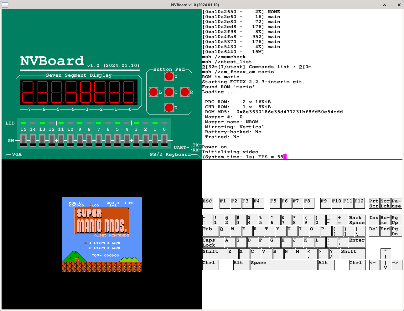
- The top layer is applications, such as Super Mario, which run in RT-Thread in a threaded manner.
- RT-Thread provides management of several resources, including physical memory, threads, etc.
- RT-Thread can also manage many resources, such as files, etc., which are currently not used in our computer system.
- AM runtime environment provides functional abstraction of TRM, IOE and CTE to support RT-Thread running on bare metal
- The RISC-V instruction set provides specific instructions, MMIO mechanisms and exception handling mechanisms to implement specific functions such as AM's TRM, IOE and CTE.
- NPC implements the functions of the RISC-V instruction set
- ysyxSoC integrates NPC, allowing NPC to communicate with various device controllers through the bus in the SoC
- NVBoard simulates the functionality of the development board, provides the physical implementation of the device, and interacts with the device controller through pins
Update RT-Thread
We added the function of integrating other AM programs to RT-Thread at 2024/01/18 20:00:00. If you obtained the code of rt-thread-am before the above time, please obtain the new version of the code:
cd rt-thread-am
git pull origin master
Run other AM programs through RT-Thread
Refer to the optional task "Running AM programs on RT-Thread" in PA4 Phase 1 and try to start other AM programs such as Super Mario through RT-Thread in riscv32e-ysyxsoc .
ChipLink - Inter-chip bus protocol
All the device controllers are located within the same SoC, thus occupying a certain area of the silicon die. If the device controllers are complex (such as modern DDR controllers), it will incur considerable die cost. In fact, we can extend the bus outside of the chip: two chips can communicate with each other following the same communication protocol. In this way, our designed chip can access devices on other chip products, which, on one hand, does not occupy our die area, thereby saving die cost, and on the other hand, can also reduce the complexity of verification and die risk, since the functions on the chip products have been thoroughly verified.
If the peer chip is an FPGA, we can also gain flexible expansion capabilities: by programming the device controllers into the FPGA, the chip can access these devices through the inter-chip bus protocol. Even if there are bugs in the device controllers, it won't lead to catastrophic consequences; it only requires reprogramming the FPGA after fixing the bugs.
However, these interfaces will occupy the chip's pins. Considering an AXI bus with both address and data widths of 32 bits, the signals araddr, awaddr, rdata, and wdata alone would occupy 128 pins. Along with various control signals, the total comes to about 150 pins; if the data width is 64 bits, then it would require over 200 pins in total. Therefore, if we directly connect the AXI bus to external components, it is likely that we would need to adopt a more expensive packaging solution, which contradicts the original intention of saving costs.
To send AXI requests externally using fewer pins, time-division multiplexing of the pins is necessary: by decomposing the AXI request signals and transmitting a portion of them at a time, a complete AXI request can be transmitted over multiple cycles. For example, if only 32 pins are used, we could agree to transmit a 32-bit write address at time T0, a 32-bit write data at time T1, and other control signals at time T2. If the peer chip also follows the same agreement, it can reassemble the information received from the 32 pins over these three cycles into an AXI write request, thereby achieving the effect of transmitting an AXI write request to another chip over three cycles.
This agreement essentially constitutes a set of inter-chip bus protocols, which stipulates the details of transmitting AXI requests externally through time-division multiplexing. For ease of description, we refer to the inter-chip bus protocol as the outer layer protocol and the bus protocol that is decomposed and transmitted as the inner layer protocol. For example, in the scenario described above, AXI serves as the inner layer protocol during inter-chip transmission. Of course, the inner layer protocol does not have to be AXI; requests from other protocols can also be decomposed and transmitted.
For instance, the inter-chip bus protocol ChipLink can use TileLink as its inner layer protocol for inter-chip transmission. Similar to AXI, TileLink is also full-duplex, meaning that the sender and receiver can transmit information on the channel simultaneously. Therefore, ChipLink is designed to be full-duplex as well. In a single direction, in addition to 32 data signals, there are also signals for clock, reset, and valid. The standard ChipLink protocol requires 70 pins, which is significantly fewer than what would be needed if TileLink, as the inner layer protocol, were to be transmitted externally by itself.
Indeed, the number of pins required by ChipLink can be further reduced by decreasing the width of the data signals. For example, when the data width is reduced to 8 bits, the ChipLink protocol only needs to occupy 22 pins. However, this reduction comes at the cost of transmission bandwidth: transmitting a request from the inner layer protocol would take more cycles, thus decreasing the amount of effective data transmitted per unit of time. If the application scenario does not demand high bandwidth, this approach can be a way to save on chip packaging costs.
ChipLink offers an open-source implementation, but it only supports TileLink as its inner layer protocol. However, we can utilize the adapter bridges in the rocket-chip project to first convert AXI requests into TileLink requests. Then, through the ChipLink protocol, TileLink requests can be transmitted to the peer chip. After the peer chip reassembles the TileLink requests according to the ChipLink protocol, it can convert the TileLink requests back into AXI requests via an adapter bridge, thereby achieving inter-chip transmission of AXI requests.
The ysyxSoC integrates the open-source implementation of ChipLink mentioned above and simulates a scenario where it is connected to a peer FPGA chip via ChipLink. The simulated peer FPGA chip contains a memory of 1GB, and ysyxSoC maps this space into the CPU's address space 0xc000_0000~0xffff_ffff. In actual use, what devices are contained within this address space is programmable, meaning that we can fully leverage the programmability of the FPGA. By updating the FPGA's bitstream file, different devices can be connected to this address space.
get new code
We have added ysyxSoCFull.v after opening ChipLink. If you obtain the code of ysyxSoC before 2024/01/11 14:15:00, please obtain the new version of the code:
cd ysyxSoC
git pull origin ysyx6
Access the resources of the peer chip through ChipLink
ysyxSoC does not open ChipLink by default, so you need to open ChipLink as follows for testing:
- If you choose Verilog, ysyxSoC provides pre-generated
.vfiles, just useysyxSoC/genreated/ysyxSoCFull-ChipLink.vas the top level for simulation - If you choose Chisel, you need to modify
hasChipLinkvariable totruein theysySoCFullclass ofysyxSoC/soc/SoC.scala, regenerateysySoCFull.vand simulate it.
However, ChipLink's code requires that the reset signal at the top level of the simulation must be maintained for at least 10 cycles. You need to check whether your simulation code meets this condition.
After opening ChipLink, test the above address space through mem-test . Since the focus of the test is to check whether the NPC can access the peer resources through ChipLink, we do not have to test the entire address space, but only need to test the access to a small section of storage space ( Such as 4KB) is sufficient.
Since the implementation of ChipLink is more complex, adding ChipLink will generate more Verilog code, which will significantly reduce the simulation efficiency. Therefore, subsequent experiments do not require you to open ChipLink. After passing the current test, you can turn off ChipLink.